CD74HCT4053E Description
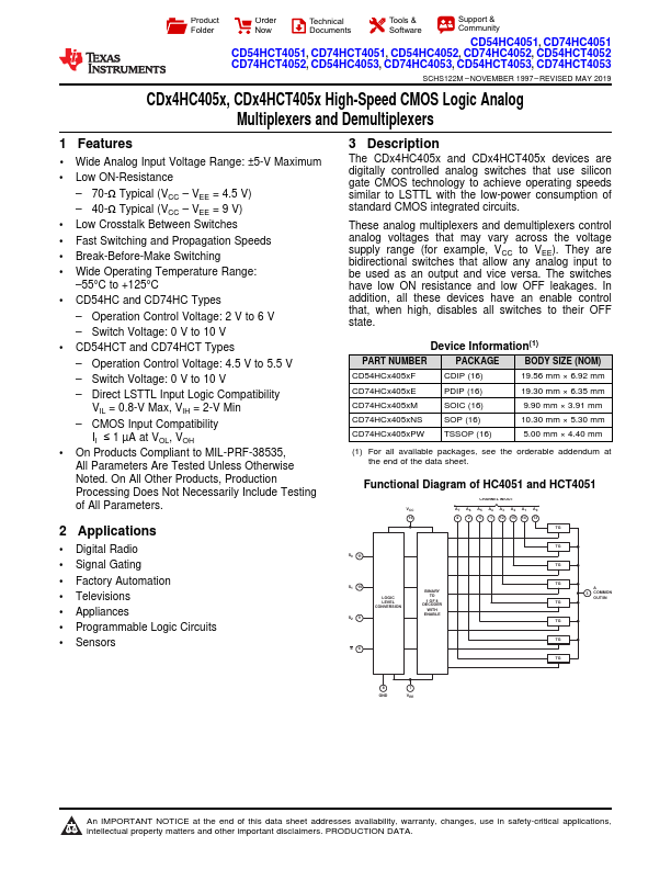
The CDx4HC405x and CDx4HCT405x devices are digitally controlled analog switches that use silicon gate CMOS technology to achieve operating speeds similar to LSTTL with the low-power consumption of standard CMOS integrated circuits. These analog multiplexers and demultiplexers control analog voltages that may vary across the voltage supply range (for example, VCC to VEE). They are bidirectional switches that allow...
CD74HCT4053E Key Features
- 1 Wide Analog Input Voltage Range: ±5-V Maximum
- Low ON-Resistance
- 70-Ω Typical (VCC
- VEE = 4.5 V)
- 40-Ω Typical (VCC
- VEE = 9 V)
- Low Crosstalk Between Switches
- Fast Switching and Propagation Speeds
- Break-Before-Make Switching
- Wide Operating Temperature Range: -55°C to +125°C