CD74HCT4075 Description
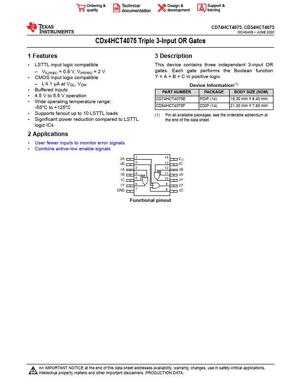
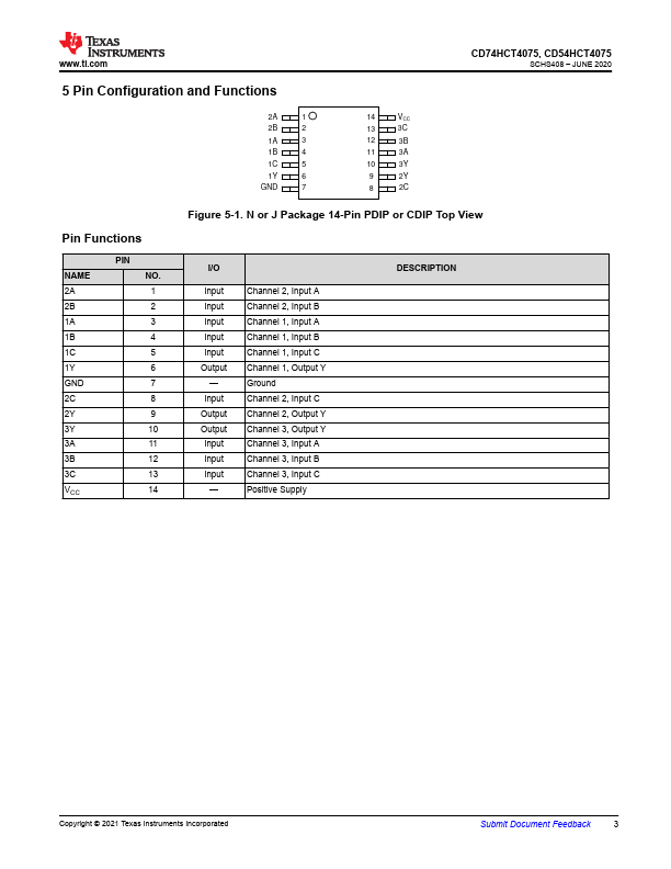
This device contains three independent 3-input OR gates. Each gate performs the Boolean function Y = A + B + C in positive logic. CD74HCT4075, CD54HCT4075 SCHS408 JUNE 2020 .ti.
CD74HCT4075 Key Features
- LSTTL input logic patible
- VIL(max) = 0.8 V, VIH(min) = 2 V
- CMOS input logic patible
- II ≤ 1 µA at VOL, VOH
- Buffered inputs
- 4.5 V to 5.5 V operation
- Wide operating temperature range
- 55°C to +125°C
- Supports fanout up to 10 LSTTL loads
- Significant power reduction pared to LSTTL
CD74HCT4075 Applications
- User fewer inputs to monitor error signals