Datasheet4U Logo Datasheet4U.com

CDC1104 - 1 to 4 Configurable Clock Buffer

Description

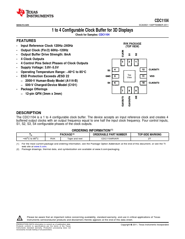
The CDC1104 is a 1 to 4 configurable clock buffer.

The device accepts an input reference clock and creates 4 buffered output clocks with an output frequency equal to one half the input clock frequency.

Four control inputs, S1, S2, S3, S4 configurable phases of the clock outputs.

40°C to

Features

  • 1.
  • Input Reference Clock 120Hz.
  • 240Hz.
  • Output Clock (Fin/2) 60Hz.
  • 120Hz.
  • Output Buffer Drive Strength: 8mA.
  • 4 Clock Outputs.
  • 4 Control Pins Select Phases of Clock Outputs.
  • Supply Voltage: 3.8V.
  • 5.5V.
  • Operating Temperature Range:.
  • 40°C to 85°C.
  • ESD Protection Exceeds JESD 22.
  • 2000-V Human-Body Model (A114-B).
  • 500-V Charged-Device Model (C101).
  • Package Offerings.

📥 Download Datasheet

Datasheet preview – CDC1104

Datasheet Details

Part number CDC1104
Manufacturer Texas Instruments
File Size 651.00 KB
Description 1 to 4 Configurable Clock Buffer
Datasheet download datasheet CDC1104 Datasheet
Additional preview pages of the CDC1104 datasheet.
Other Datasheets by Texas Instruments

Full PDF Text Transcription

Click to expand full text
www.ti.com 1 to 4 Configurable Clock Buffer for 3D Displays Check for Samples: CDC1104 CDC1104 SCAS921 – SEPTEMBER 2011 FEATURES 1 • Input Reference Clock 120Hz–240Hz • Output Clock (Fin/2) 60Hz–120Hz • Output Buffer Drive Strength: 8mA • 4 Clock Outputs • 4 Control Pins Select Phases of Clock Outputs • Supply Voltage: 3.8V–5.5V • Operating Temperature Range: –40°C to 85°C • ESD Protection Exceeds JESD 22 – 2000-V Human-Body Model (A114-B) – 500-V Charged-Device Model (C101) • Package Offerings – 12-pin QFN (3mm x 3mm) RVK PACKAGE (TOP VIEW) CLKIN S1 S2 321 S3 4 GND 5 S4 6 Top View 12 CLKOUT1 11 VDD 10 CLKOUT2 789 CLKOUT3 CLKOUT4 OE DESCRIPTION The CDC1104 is a 1 to 4 configurable clock buffer.
Published: |