Texas Instruments CDCVF855
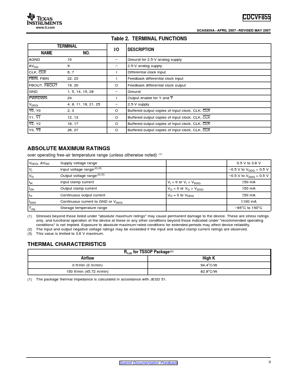
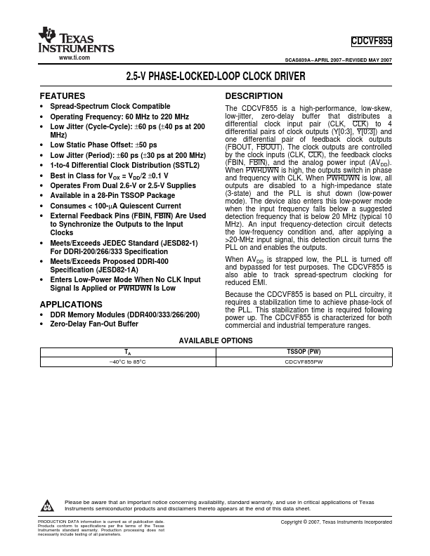
The CDCVF855 is a high-performance, low-skew, low-jitter, zero-delay buffer that distributes a differential clock input pair (CLK, CLK) to 4 differential pairs of clock outputs (Y[0:3], Y[0:3]) and one differential pair of feedback clock outputs (FBOUT, FBOUT). The clock outputs are controlled by the clock inputs (CLK, CLK), the feedback clocks (FBIN, FBIN), and the analog power input (AVDD). When PWRDWN is high, the outputs switch in phase and frequency with CLK.| Part No. | CDCVF855 |
|---|---|
| Datasheet | CDCVF855 Download |
| Manufacturer |  Texas Instruments |
| Description | 2.5-V PHASE-LOCKED-LOOP CLOCK DRIVER |
| Buy | Stock & Price |
FEATURES
● Spread-Spectrum Clock Compatible● Operating Frequency: 60 MHz to 220 MHz
● Low Jitter (Cycle-Cycle): ±60 ps (±40 ps at 200 MHz)
● Low Static Phase Offset: ±50 ps
● Low Jitter (Period): ±60 ps (±30 ps at 200 MHz)
● 1-to-4 Differential Clock Distribution (SSTL2)
● Best in Class for VOX = VDD/2 ±0.1 V
● Operates From Dual 2.6-V or 2.5-V Supplies
● Available in a 28-Pin TSSOP Package
● Consumes < 100-µA Quiescent Current
● External Feedback Pins (FBIN, FBIN) Are Used to Synchronize the Outputs to the Input Clocks
● Meets/Exceeds JEDEC Standard (JESD82-1) For DDRI-200/266/333 Specification
● Meets/Exceeds Proposed DDRI-400 Specification (JESD82-1A)
● Enters Low-Power Mode When No CLK Input Signal Is Applied or PWRDWN Is Low
APPLICATIONS
● DDR Memory Modules (DDR400/333/266/200)● Zero-Delay Fan-Out Buffer
DESCRIPTION
When PWRDWN is low, all outputs are disabled to a high-impedance state (3-state) and the PLL is shut down (low-power mode). The device also enters this low-power mode when the input frequency falls below a suggested detection frequency that is below 20 MHz (typical 10 MHz).