Datasheet4U Logo Datasheet4U.com

CSD16322Q5 Datasheet N-Channel Power MOSFET

Manufacturer: Texas Instruments

General Description

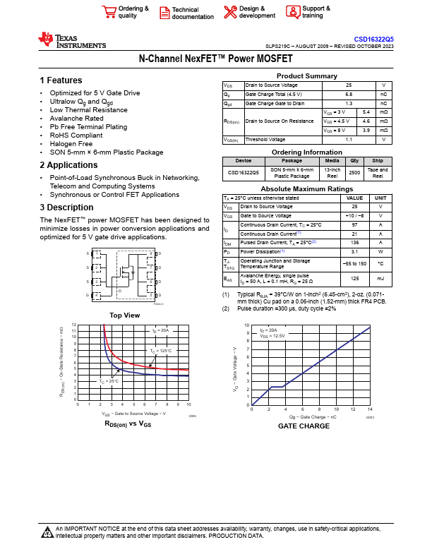
The NexFET™ power MOSFET has been designed to minimize losses in power conversion applications and optimized for 5 V gate drive applications.

S1 8D S2 7D S3 6D D G4 5D P0094-01 Top View 12 11 ID = 20A 10 9 8 TC = 125°C 7 6 5 4 3 TC = 25°C 2 1 0 0 1 2 3 4 5 6 7 8 9 10 VGS − Gate to Source Voltage − V G006 RDS(on) vs VGS Product Summary VDS Drain to Source Voltage 25 V Qg Gate Charge Total (4.5 V) 6.8 nC Qgd Gate Charge Gate to Drain 1.3 nC VGS = 3 V 5.4 mΩ RDS(on) Drain to Source On Resistance VGS = 4.5 V 4.6 mΩ VGS = 8 V 3.9 mΩ VGS(th) Threshold Voltage 1.1 V Device CSD16322Q5 Ordering Information Package Media SON 5-mm × 6-mm Plastic Package 13-Inch Reel Qty 2500 Ship Tape and Reel Absolute Maximum Ratings TA = 25°C unless otherwise stated VDS Drain to Source Voltage VALUE 25 VGS Gate to Source Voltage ID Continuous Drain Current, TC = 25°C Continuous Drain Current(1) +10 / –8 97 21 IDM Pulsed Drain Current, TA = 25°C(2) 136 PD Power Dissipation(1) 3.1 TJ, TSTG EAS Operating Junction and Storage Temperature Range Avalanche Energy, single pulse ID = 50 A, L = 0.1 mH, RG = 25 Ω –55 to 150 125 UNIT V V A A A W °C mJ (1) Typical RθJA = 39°C/W on 1-inch2 (6.45-cm2), 2-oz.

(0.071mm thick) Cu pad on a 0.06-inch (1.52-mm) thick FR4 PCB.

Overview

CSD16322Q5 SLPS219C – AUGUST 2009 – REVISED OCTOBER 2023 N-Channel NexFET™ Power MOSFET RDS(on) − On-State Resistance − mW VG − Gate Voltage − V.

Key Features

  • Optimized for 5 V Gate Drive.
  • Ultralow Qg and Qgd.
  • Low Thermal Resistance.
  • Avalanche Rated.
  • Pb Free Terminal Plating.
  • RoHS Compliant.
  • Halogen Free.
  • SON 5-mm × 6-mm Plastic Package 2.