Datasheet4U Logo Datasheet4U.com

CSD18509Q5B - Power MOSFETs

General Description

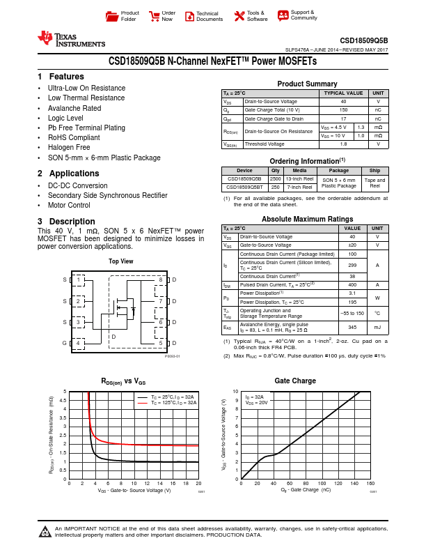
This 40 V, 1 mΩ, SON 5 x 6 NexFET™ power MOSFET has been designed to minimize losses in power conversion applications.

Top View S1 8D S2 7D S3 D G4 6D 5D P0093-01 Absolute Maximum Ratings TA = 25°C VDS Drain-to-Source Voltage VGS Gate-to-Source Voltage Continuous Drain Current (Package limited) VALUE 40 ±20 100 UNIT V V ID Continuous Drain Current (Silicon limited), TC = 25°C 299 A Continuous Drain Current(1) 38 IDM Pulsed Drain Current, TA = 25°C(2) Power Dissipation(1) PD Power Dissipation, TC = 25°C 400 A 3.1 W 195 TJ, Operating Junction and Tstg Storage Temperature Range –55 to 150 °C EAS Avalanche Energy, single pulse ID = 83, L = 0.1 mH, RG = 25 Ω 345 mJ (1) Typical RθJA = 40°C/W on a 1-inch2, 2-oz.

Cu pad on a 0.06-inch thick FR4 PCB.

Overview

Product Folder Order Now Technical Documents Tools & Software Support & Community CSD18509Q5B SLPS476A – JUNE 2014 – REVISED MAY 2017 CSD18509Q5B N-Channel NexFET™ Power MOSFETs.

Key Features

  • 1 Ultra-Low On Resistance.
  • Low Thermal Resistance.
  • Avalanche Rated.
  • Logic Level.
  • Pb Free Terminal Plating.
  • RoHS Compliant.
  • Halogen Free.
  • SON 5-mm × 6-mm Plastic Package 2.