CSD22202W15
Description
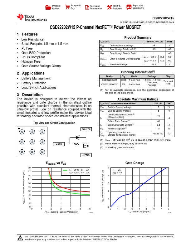
The device is designed to deliver the lowest on resistance and gate charge in the smallest outline possible with excellent Top View and Circuit Configuration G S S Source S S S Gate DDD Drain Product Summary TA = 25°C VDS Drain-to-Source Voltage Qg Gate Charge Total (–4.5 V) Qgd Gate Charge Gate-to-Drain RDS(on) Drain-to-Source On-Resistance VGS(th) Threshold Voltage TYPICAL VALUE –8 6.5 1 VGS = –2.5 V VGS = –4.5 V –0.8 14.5 10.2 UNIT V nC nC mΩ mΩ V Device CSD22202W15 CSD22202W15T.
Key Features
- 1 Low Resistance
- Small Footprint 1.5 mm × 1.5 mm
- Gate ESD Protection
- RoHS compliant
- Halogen Free
- Gate-Source Voltage Clamp