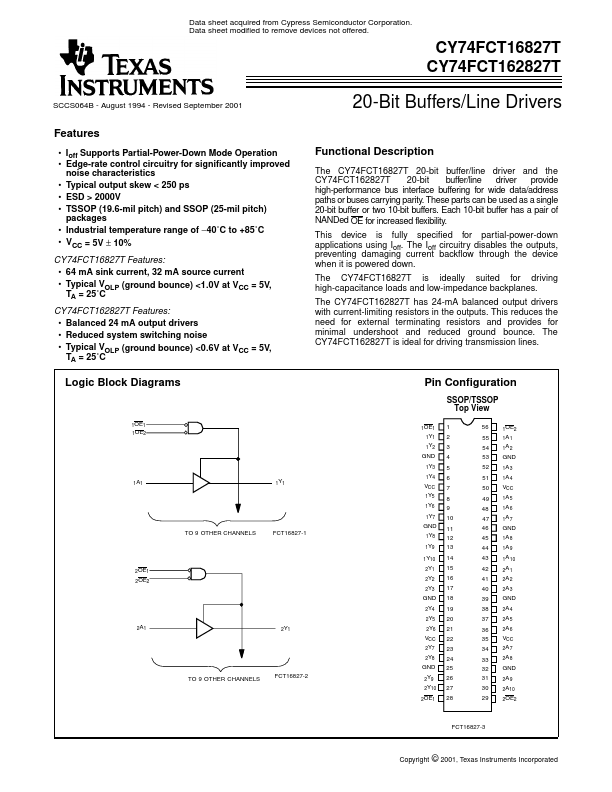
1CY74FCT162827T
Data sheet acquired from Cypress Semiconductor Corporation.
Data sheet modified to remove devices not offered.
CY74FCT16827T
CY74FCT162827T
SCCS064B - August 1994 - Revised September 2001
20-Bit Buffers/Line Drivers
Features
• Ioff Supports Partial-Power-Down Mode Operation
• Edge-rate control circuitry for significantly improved
noise characteristics
• Typical output skew < 250 ps
• ESD > 2000V
• TSSOP (19.6-mil pitch) and SSOP (25-mil pitch)
packages
• Industrial temperature range of −40˚C to +85˚C
• VCC = 5V ± 10%
CY74FCT16827T Features:
• 64 mA sink current, 32 mA source current
• Typical VOLP (ground bounce) <1.0V at VCC = 5V,
TA = 25˚C
CY74FCT162827T Features:
• Balanced 24 mA output drivers
• Reduced system switching noise
• Typical VOLP (ground bounce) <0.6V at VCC = 5V,
TA = 25˚C
Functional Description
The CY74FCT16827T 20-bit buffer/line driver and the
CY74FCT162827T 20-bit buffer/line driver provide
high-performance bus interface buffering for wide data/address
paths or buses carrying parity. These parts can be used as a single
20-bit buffer or two 10-bit buffers. Each 10-bit buffer has a pair of
NANDed OE for increased flexibility.
This device is fully specified for partial-power-down
applications using Ioff. The Ioff circuitry disables the outputs,
preventing damaging current backflow through the device
when it is powered down.
The CY74FCT16827T is ideally suited for driving
high-capacitance loads and low-impedance backplanes.
The CY74FCT162827T has 24-mA balanced output drivers
with current-limiting resistors in the outputs. This reduces the
need for external terminating resistors and provides for
minimal undershoot and reduced ground bounce. The
CY74FCT162827T is ideal for driving transmission lines.
Logic Block Diagrams
1OE1
1OE2
1A1
1Y1
2OE1
2OE2
TO 9 OTHER CHANNELS
FCT16827-1
2A1 2Y1
TO 9 OTHER CHANNELS
FCT16827-2
Pin Configuration
SSOP/TSSOP
Top View
1OE1
1Y1
1Y2
GND
1Y3
1Y4
VCC
1Y5
1Y6
1Y7
GND
1Y8
1Y9
1Y10
2Y1
2Y2
2Y3
GND
2Y4
2Y5
2Y6
VCC
2Y7
2Y8
GND
2Y9
2Y10
2OE1
1
2
3
4
5
6
7
8
9
10
11
12
13
14
15
16
17
18
19
20
21
22
23
24
25
26
27
28
56 1OE2
55 1A1
54 1A2
53 GND
52 1A3
51 1A4
50 VCC
49 1A5
48 1A6
47 1A7
46 GND
45 1A8
44 1A9
43 1A10
42 2A1
41 2A2
40 2A3
39 GND
38 2A4
37 2A5
36 2A6
35 VCC
34 2A7
33 2A8
32 GND
31 2A9
30 2A10
29 2OE2
FCT16827-3
Copyright © 2001, Texas Instruments Incorporated