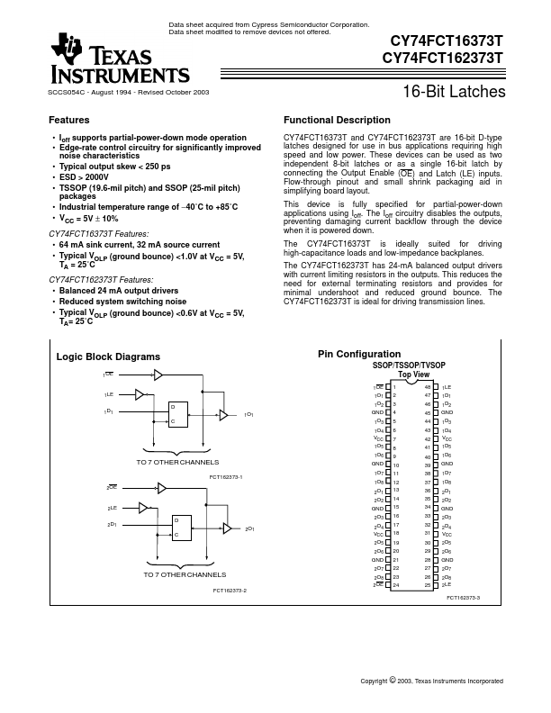
CY74FCT16373T
CY74FCT162373T
Pin Description
Name
D
LE
OE
O
Description
Data Inputs
Latch Enable Inputs (Active HIGH)
Output Enable Inputs (Active LOW)
Three-State Outputs
Function Table[1]
Inputs
D LE
HH
LH
XL
XX
OE
L
L
L
H
Outputs
O
H
L
Q0
Z
Maximum Ratings[2, 3]
(Above which the useful life may be impaired. For user
guidelines, not tested.)
Storage Temperature ...................... Com’l −55°C to +125°C
Ambient Temperature with
Power Applied................................. Com’l −55°C to +125°C
DC Input Voltage .................................................−0.5V to +7.0V
DC Output Voltage ..............................................−0.5V to +7.0V
DC Output Current
(Maximum Sink Current/Pin) ...........................−60 to +120 mA
Power Dissipation .......................................................... 1.0W
Static Discharge Voltage............................................>2001V
(per MIL-STD-883, Method 3015)
Operating Range
Range
Industrial
Ambient
Temperature
−40°C to +85°C
VCC
5V ± 10%
Electrical Characteristics Over the Operating Range
Parameter
Description
VIH
VIL
VH
VIK
IIH
IIL
IOZH
Input HIGH Voltage
Input LOW Voltage
Input Hysteresis[5]
Input Clamp Diode Voltage
Input HIGH Current
Input LOW Current
High Impedance Output Current
(Three-State Output pins)
IOZL High Impedance Output Current
(Three-State Output pins)
IOS Short Circuit Current[6]
IO Output Drive Current[6]
IOFF Power-Off Disable
Test Conditions
VCC=Min., IIN=−18 mA
VCC=Max., VI=VCC
VCC=Max., VI=GND
VCC=Max., VOUT=2.7V
VCC=Max., VOUT=0.5V
VCC=Max., VOUT=GND
VCC=Max., VOUT=2.5V
VCC=0V, VOUT≤4.5V[7]
Min.
2.0
Typ.[4]
100
−0.7
Max.
0.8
−1.2
±1
±1
±1
Unit
V
V
mV
V
µA
µA
µA
±1 µA
−80 −140 −200 mA
−50 −180 mA
±1 µA
Output Drive Characteristics for CY74FCT16373T
Parameter
Description
Test Conditions
Min. Typ.[4] Max. Unit
VOH Output HIGH Voltage
VCC=Min., IOH=−3 mA
2.5 3.5
V
VCC=Min., IOH=−15 mA
2.4 3.5
V
VCC=Min., IOH=−32 mA
2.0 3.0
V
VOL Output LOW Voltage
VCC=Min., IOL=64 mA
0.2 0.55 V
Notes:
1. H = HIGH Voltage Level. L = LOW Voltage Level. X = Don’t Care. Z = High Impedance. Q0=Previous state of flip-flop.
2. Operation beyond the limits set forth may impair the useful life of the device. Unless otherwise noted, these limits are over the operating free-air temperature
range.
3. Unused inputs must always be connected to an appropriate logic voltage level, preferably either VCC or ground.
4. Typical values are at VCC=5.0V, TA= +25˚C ambient.
5. This parameter is specified but not tested.
6. Not more than one output should be shorted at a time. Duration of short should not exceed one second. The use of high-speed test apparatus and/or sample
and hold techniques are preferable in order to minimize internal chip heating and more accurately reflect operational values. Otherwise prolonged shorting of
a high output may raise the chip temperature well above normal and thereby cause invalid readings in other parametric tests. In any sequence of parameter
tests, IOS tests should be performed last.
7. Tested at +25˚C.
2