DAC101C081Q
Overview
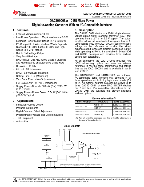
The DAC101C081 device is a 10-bit, single channel, voltage-output digital-to-analog converter (DAC) that operates from a 2.7 V to 5.5 V supply. The output amplifier allows rail-to-rail output swing and has an 6µsec settling time.
- 1 Ensured Monotonicity to 10-bits
- Low Power Operation: 156-µA maximum at 3.3 V
- Extended Power Supply Range (2.7 V to 5.5 V)
- I2C-Compatible 2-Wire Interface Which Supports Standard (100-kHz), Fast (400-kHz), and HighSpeed (3.4-MHz) Modes
- Rail-to-Rail Voltage Output
- Very Small Package
- DAC101C081Q is AEC Q100 Grade 1 Qualified and Manufactured on Automotive Grade Flow
- Resolution: 10 Bits
- INL: ±2 LSB (Maximum)
- DNL: +0.3/-0.2 LSB (Maximum)