LM3410-Q1
LM3410-Q1 is Constant-Current Boost and SEPIC LED Driver manufactured by Texas Instruments.
- Part of the LM3410 comparator family.
- Part of the LM3410 comparator family.
Product Folder
Sample & Buy
Technical Documents
Tools & Software
Support & munity
LM3410, LM3410-Q1
SNVS541H
- OCTOBER 2007
- REVISED AUGUST 2016
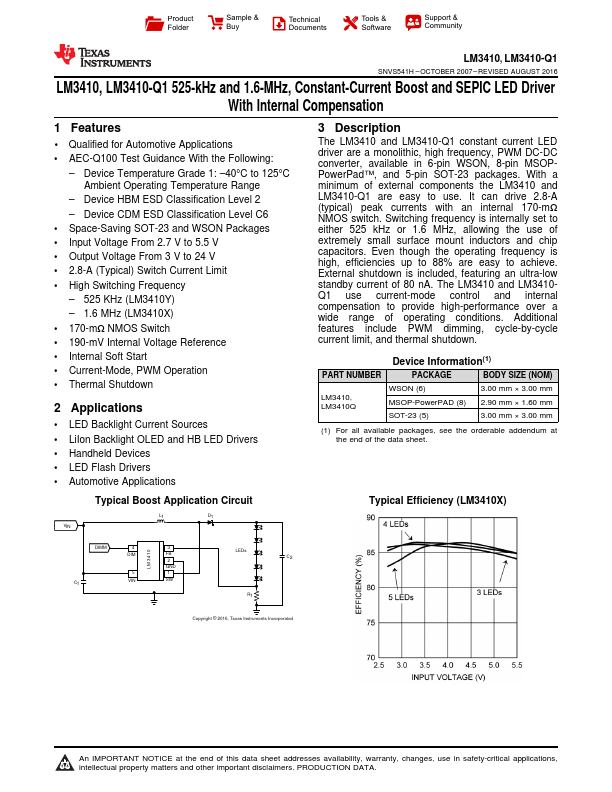
LM3410, LM3410-Q1 525-k Hz and 1.6-MHz, Constant-Current Boost and SEPIC LED Driver With Internal pensation
1 Features
- 1 Qualified for Automotive Applications
- AEC-Q100 Test Guidance With the Following:
- Device Temperature Grade 1:
- 40°C to 125°C Ambient Operating Temperature Range
- Device HBM ESD Classification Level 2
- Device CDM ESD Classification Level C6
- Space-Saving SOT-23 and WSON Packages
- Input Voltage From 2.7 V to 5.5 V
- Output Voltage From 3 V to 24 V
- 2.8-A (Typical) Switch Current Limit
- High Switching Frequency
- 525 KHz (LM3410Y)
- 1.6 MHz (LM3410X)
- 170-mΩ NMOS Switch
- 190-m V Internal Voltage Reference
- Internal Soft Start
- Current-Mode, PWM Operation
- Thermal Shutdown
2...