Datasheet4U Logo Datasheet4U.com

LM5114 - Low-Side Gate Driver

General Description

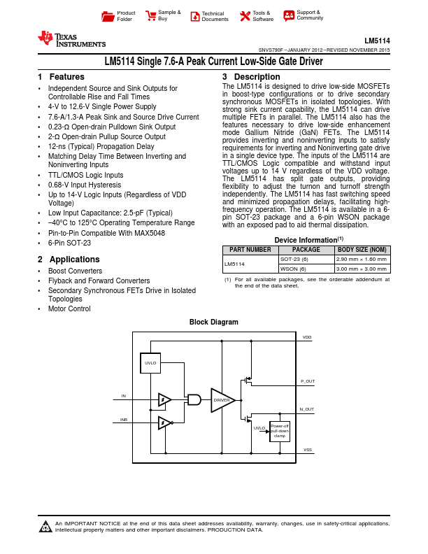
The LM5114 is designed to drive low-side MOSFETs in boost-type configurations or to drive secondary synchronous MOSFETs in isolated topologies.

With strong sink current capability, the LM5114 can drive multiple FETs in parallel.

Key Features

  • 1 Independent Source and Sink Outputs for Controllable Rise and Fall Times.
  • 4-V to 12.6-V Single Power Supply.
  • 7.6-A/1.3-A Peak Sink and Source Drive Current.
  • 0.23-Ω Open-drain Pulldown Sink Output.
  • 2-Ω Open-drain Pullup Source Output.
  • 12-ns (Typical) Propagation Delay.
  • Matching Delay Time Between Inverting and Noninverting Inputs.
  • TTL/CMOS Logic Inputs.
  • 0.68-V Input Hysteresis.
  • Up to 14-V Logic Inputs (Reg.

📥 Download Datasheet

Full PDF Text Transcription for LM5114 (Reference)

Note: Below is a high-fidelity text extraction (approx. 800 characters) for LM5114. For precise diagrams, and layout, please refer to the original PDF.

Product Folder Sample & Buy Technical Documents Tools & Software Support & Community LM5114 SNVS790F – JANUARY 2012 – REVISED NOVEMBER 2015 LM5114 Single 7.6-A Peak Curre...

View more extracted text
– JANUARY 2012 – REVISED NOVEMBER 2015 LM5114 Single 7.6-A Peak Current Low-Side Gate Driver 1 Features •1 Independent Source and Sink Outputs for Controllable Rise and Fall Times • 4-V to 12.6-V Single Power Supply • 7.6-A/1.3-A Peak Sink and Source Drive Current • 0.23-Ω Open-drain Pulldown Sink Output • 2-Ω Open-drain Pullup Source Output • 12-ns (Typical) Propagation Delay • Matching Delay Time Between Inverting and Noninverting Inputs • TTL/CMOS Logic Inputs • 0.68-V Input Hysteresis • Up to 14-V Logic Inputs (Regardless of VDD Voltage) • Low Input Capacitance: 2.