LMK01801
Description
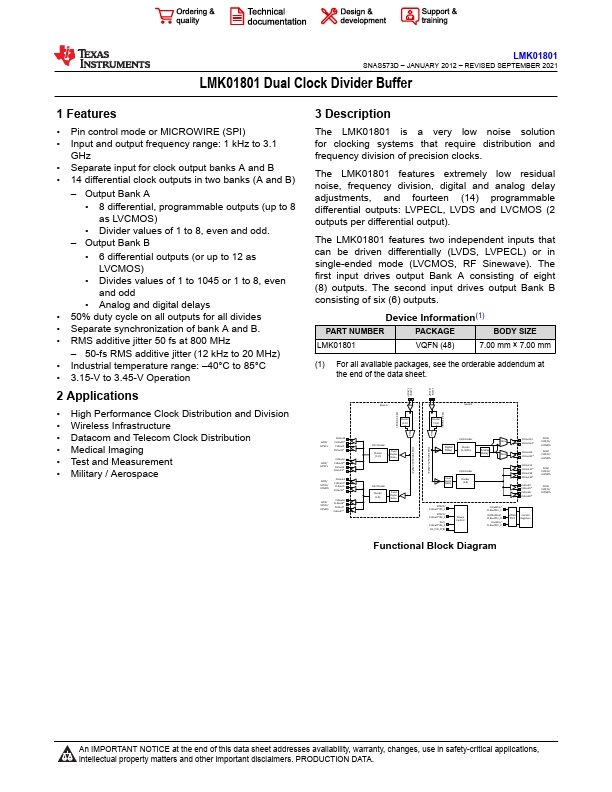
The LMK01801 is a very low noise solution for clocking systems that require distribution and frequency division of precision clocks. The LMK01801 features extremely low residual noise, frequency division, digital and analog delay adjustments, and fourteen (14) programmable differential outputs: LVPECL, LVDS and LVCMOS (2 outputs per differential output).
Key Features
- Pin control mode or MICROWIRE (SPI)
- Input and output frequency range: 1 kHz to 3.1 GHz
- Separate input for clock output banks A and B
- 14 differential clock outputs in two banks (A and B) - Output Bank A
- 8 differential, programmable outputs (up to 8 as LVCMOS)
- Divider values of 1 to 8, even and odd. - Output Bank B
- 6 differential outputs (or up to 12 as LVCMOS)
- Divides values of 1 to 1045 or 1 to 8, even and odd
- Analog and digital delays
- 50% duty cycle on all outputs for all divides