LP5900 Overview
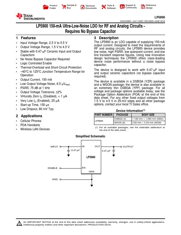
The LP5900 is an LDO capable of supplying 150-mA output current. Designed to meet the requirements of RF and analog circuits, the LP5900 device provides low noise, high PSRR, low quiescent current, and low line transient response figures. Using new innovative design techniques the LP5900 offers class-leading device noise performance without a noise bypass capacitor.
LP5900 Key Features
- 1 Input Voltage Range, 2.5 V to 5.5 V
- Output Voltage Range, 1.5 V to 4.5 V
- Stable with 0.47-μF Ceramic Input and Output
- No Noise Bypass Capacitor Required
- Logic Controlled Enable
- Thermal-Overload and Short-Circuit Protection
- Output Current, 150 mA
- Low Output Voltage Noise, 6.5 μVRMS
- PSRR, 75 dB at 1 kHz
- Output Voltage Tolerance, ±2%