LP85571 Overview
Description
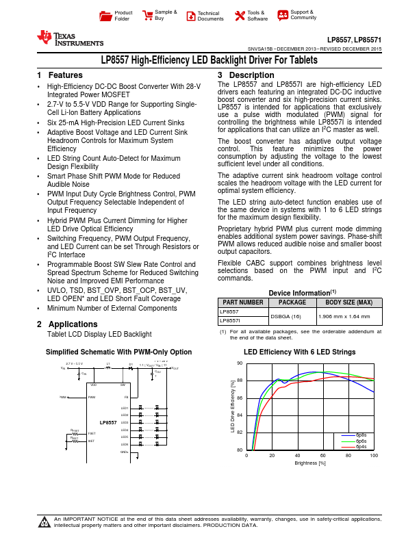
The LP8557 and LP8557I are high-efficiency LED drivers each featuring an integrated DC-DC inductive boost converter and six high-precision current sinks. LP8557 is intended for applications that exclusively use a pulse width modulated (PWM) signal for controlling the brightness while LP8557I is intended for applications that can utilize an I2C master as well.
Key Features
- 1 High-Efficiency DC-DC Boost Converter With 28-V Integrated Power MOSFET
- 2.7-V to 5.5-V VDD Range for Supporting SingleCell Li-Ion Battery Applications
- Six 25-mA High-Precision LED Current Sinks
- Adaptive Boost Voltage and LED Current Sink Headroom Controls for Maximum System Efficiency
- LED String Count Auto-Detect for Maximum Design Flexibility
- Smart Phase Shift PWM Mode for Reduced Audible Noise
- PWM Input Duty Cycle Brightness Control, PWM Output Frequency Selectable Independent of Input Frequency
- Hybrid PWM Plus Current Dimming for Higher LED Drive Optical Efficiency
- Switching Frequency, PWM Output Frequency, and LED Current can be set Through Resistors or I2C Interface
- Programmable Boost SW Slew Rate Control and Spread Spectrum Scheme for Reduced Switching Noise and Improved EMI Performance