Datasheet4U Logo Datasheet4U.com

SN54LV367A - HEX BUFFERS AND LINE DRIVER

Description

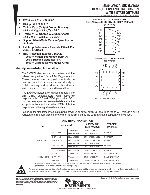
The ’LV367A devices are hex buffers and line drivers designed for 2-V to 5.5-V VCC operation.

These devices are designed specifically to improve both the performance and density of 3-state memory address drivers, clock drivers, and bus-oriented receivers and transmitters.

📥 Download Datasheet

Full PDF Text Transcription (Reference)

The following content is an automatically extracted verbatim text from the original manufacturer datasheet and is provided for reference purposes only.

View original datasheet text
D 2-V to 5.5-V VCC Operation D Max tpd of 7 ns at 5 V D Typical VOLP (Output Ground Bounce) <0.8 V at VCC = 3.3 V, TA = 25°C D Typical VOHV (Output VOH Undershoot) >2.3 V at VCC = 3.3 V, TA = 25°C D Support Mixed-Mode Voltage Operation on All Ports D Latch-Up Performance Exceeds 100 mA Per JESD 78, Class II D ESD Protection Exceeds JESD 22 − 2000-V Human-Body Model (A114-A) − 200-V Machine Model (A115-A) − 1000-V Charged-Device Model (C101) SN54LV367A, SN74LV367A HEX BUFFERS AND LINE DRIVERS WITH 3ĆSTATE OUTPUTS SCLS398G − APRIL 1998 − REVISED APRIL 2005 SN54LV367A . . . J OR W PACKAGE SN74LV367A . . . D, DB, DGV, NS, OR PW PACKAGE (TOP VIEW) 1OE 1 1A1 2 1Y1 3 1A2 4 1Y2 5 1A3 6 1Y3 7 GND 8 16 VCC 15 2OE 14 2A2 13 2Y2 12 2A1 11 2Y1 10 1A4 9 1Y4 SN54LV367A . . .
Published: |