SN55LBC173
SN55LBC173 is QUADRUPLE LOW-POWER DIFFERENTIAL RECEIVER manufactured by Texas Instruments.
description
The SN55LBC173 is a monolithic quadruple differential line receiver with 3-state outputs designed to meet the requirements of the EIA standards RS-422-A, RS-423-A, RS-485, and CCITT V.11. This device is optimized for balanced multipoint bus transmission at data rates up to and exceeding 10 million bits per second. The four receivers share two ORed enable inputs, one active when high, the other active when low. Each receiver features high input impedance, input hysteresis for increased noise immunity, and input sensitivity of ± 200 m V over a mon-mode input voltage range of 12 V to
- 7 V. Fail-safe design ensures that if the inputs are open circuited, the output is always high. The SN55LBC173 is designed using the Texas Instruments proprietary Lin Bi CMOS™ technology that provides low power consumption, high switching speeds, and robustness.
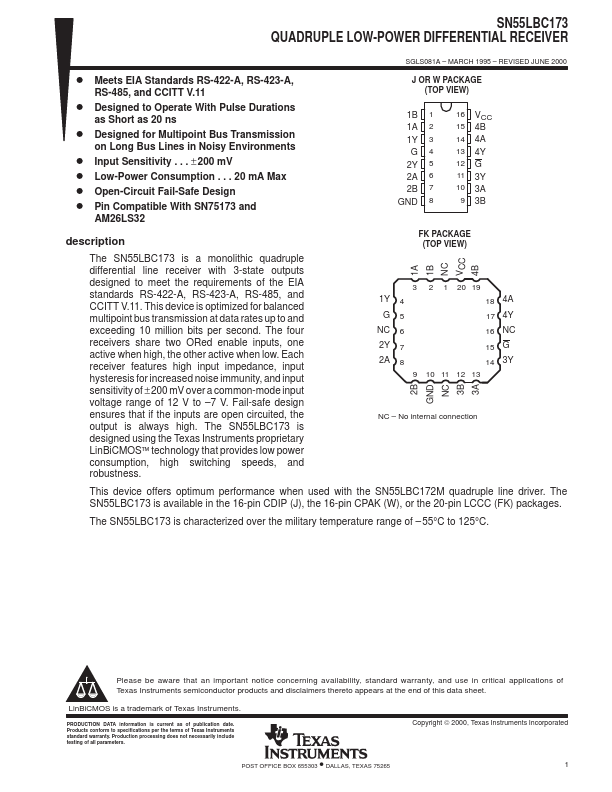
FK PACKAGE (TOP VIEW)
1A 1B NC VCC 4B
3 2 1 20 19
1Y 4
18 4A
G5
17 4Y
NC 6
16 NC
2Y 7
15 G
2A 8
14 3Y
9 10 11 12 13
2B GND
NC 3B 3A
- No internal connection
This device offers optimum performance when used with the SN55LBC172M quadruple line driver. The SN55LBC173 is available in the 16-pin CDIP (J), the 16-pin CPAK (W), or the 20-pin LCCC (FK) packages.
The SN55LBC173 is characterized over the military temperature range of
- 55°C to 125°C.
Please be aware that an important notice concerning availability, standard warranty, and use in critical applications of Texas Instruments semiconductor products and disclaimers thereto appears at the end of this data sheet.
Lin Bi CMOS is a trademark of Texas Instruments.
PRODUCTION DATA information is current as of publication date. Products conform to specifications per the terms of Texas Instruments standard warranty. Production processing does not necessarily include testing of all parameters.
Copyright © 2000, Texas Instruments Incorporated
- POST OFFICE BOX 655303 DALLAS, TEXAS 75265
SN55LBC173 QUADRUPLE LOW-POWER DIFFERENTIAL RECEIVER
SGLS081A
-...