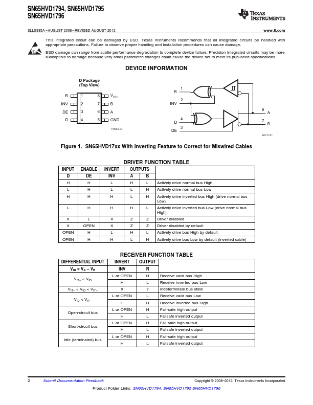
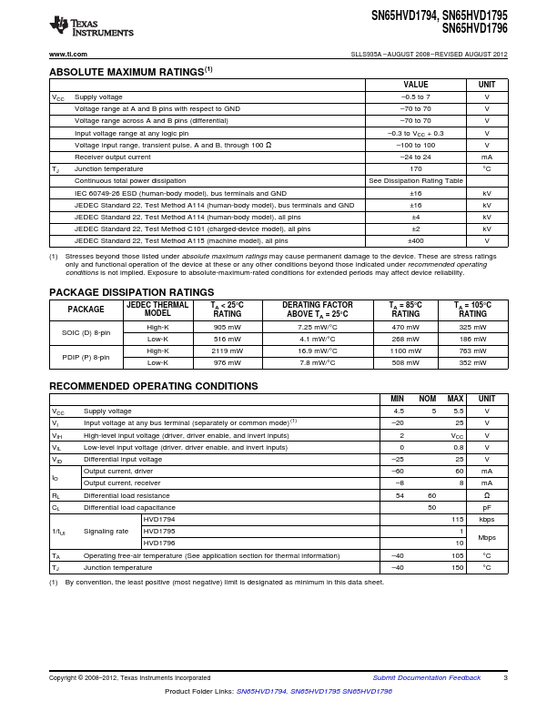
SN65HVD1794 Description
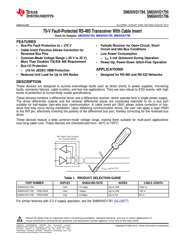
These devices are designed to survive overvoltage faults such as direct shorts to power supplies, mis-wiring faults, connector failures, cable crushes, and tool mis-applications. They are also robust to ESD events, with high levels of protection to human-body model specifications. These devices bine a differential driver and a differential receiver, which operate from a single power supply.
SN65HVD1794 Key Features
- Bus-Pin Fault Protection to > ±70 V
- mon-Mode Voltage Range (-20 V to 25 V)
- Bus I/O Protection
- ±16 kV JEDEC HBM Protection
- Reduced Unit Load for Up to 256 Nodes
- Failsafe Receiver for Open-Circuit, ShortCircuit and Idle-Bus Conditions
- Low Power Consumption
- ICC 5 mA Quiescent During Operation
- Power-Up, Power-Down Glitch-Free Operation
SN65HVD1794 Applications
- Designed for RS-485 and RS-422 Networks