SN65LBC173 Overview
Description
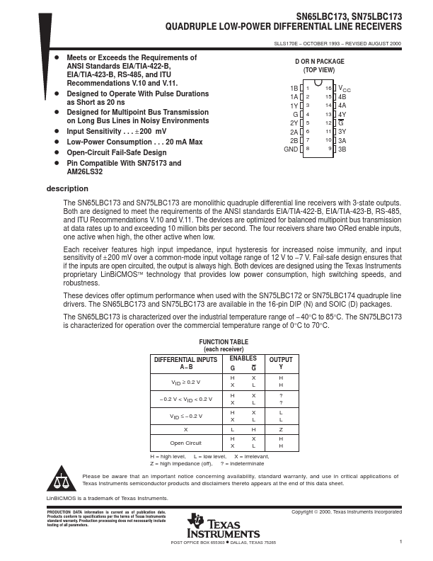
The SN65LBC173 and SN75LBC173 are monolithic quadruple differential line receivers with 3-state outputs. Both are designed to meet the requirements of the ANSI standards EIA/TIA-422-B, EIA/TIA-423-B, RS-485, and ITU Recommendations V.10 and V.11.
Key Features
- Fail-safe design ensures that if the inputs are open circuited, the output is always high
- These devices offer optimum performance when used with the SN75LBC172 or SN75LBC174 quadruple line drivers
- The SN65LBC173 and SN75LBC173 are available in the 16-pin DIP (N) and SOIC (D) packages
- The SN65LBC173 is characterized over the industrial temperature range of -40°C to 85°C
- The SN75LBC173 is characterized for operation over the commercial temperature range of 0°C to 70°C