• Part: SN65LVDS122
  • Description: LVDS CROSSPOINT SWITCH
  • Manufacturer: Texas Instruments
  • Size: 1.20 MB
Download SN65LVDS122 Datasheet PDF
SN65LVDS122 page 2
Page 2
SN65LVDS122 page 3
Page 3

SN65LVDS122 Datasheet Text

.ti. SN65LVDS122 SN65LVDT122 SLLS525B - MAY 2002 - REVISED JUNE 2004 1.5-Gbps 2 × 2 LVDS CROSSPOINT SWITCH Features - Designed for Signaling Rates (1) Up To 1.5 Gbps - Total Jitter < 65 ps - Pin-patible With SN65LVDS22 and SN65LVDM22 - 25 mV of Receiver Input Threshold Hysteresis Over 0-V to 4-V mon-Mode Range - Inputs Electrically patible With CML, LVPECL and LVDS Signal Levels - Propagation Delay Times, 900 ps Maximum - LVDT Integrates 110-Ω Terminating Resistor - Offered in SOIC and TSSOP APPLICATIONS - 10-G (OC-192) Optical Modules - 622-MHz Central Office Clock Distribution - Wireless Basestations - Low Jitter Clock Repeater/Multiplexer - Protection Switching for Serial Backplanes (1) The signlaing rate of a line is the number of voltage transitions that are made per second expressed in the units bps (bits per second). FUNCTIONAL DIAGRAM 1DE DESCRIPTION 
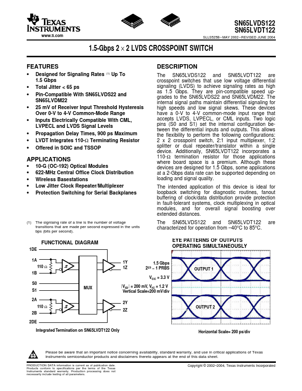
The SN65LVDS122 and SN65LVDT122 are crosspoint switches that use low voltage differential signaling (LVDS) to achieve signaling rates as high as 1.5 Gbps. They are pin-patible speed upgrades to the SN65LVDS22 and SN65LVDM22. The internal signal paths maintain differential signaling for high speeds and low signal skews. These devices have a 0-V to 4-V mon-mode input range that accepts LVDS, LVPECL, or CML inputs. Two logic pins (S0 and S1) set the internal configuration between the differential inputs and outputs. This allows the flexibility to perform the following configurations: 2 x 2 crosspoint switch, 2:1 input multiplexer, 1:2 splitter or dual repeater/translator within a single device. Additionally, SN65LVDT122 incorporates a 110-Ω termination resistor for those applications where board space is a premium. Although these devices are designed for 1.5 Gbps, some applications at a 2-Gbps...