SN74AHC126 Datasheet Text
SN54AHC126, SN74AHC126
SCLS257N
- DECEMBER 1995
- REVISED FEBRUARY 2024
SNx4AHC126 Quadruple Bus Buffer Gates with 3-State Outputs
1 Features
- Operating range 2V to 5.5V VCC
- Low delay, 3.8 ns (typical with 5-V supply)
- Latch-up performance exceeds 250mA per JESD 17
2 Applications
- Drive indicator LEDs
- Drive transmission lines with logic
- Enable or disable a digital signal
3 Description
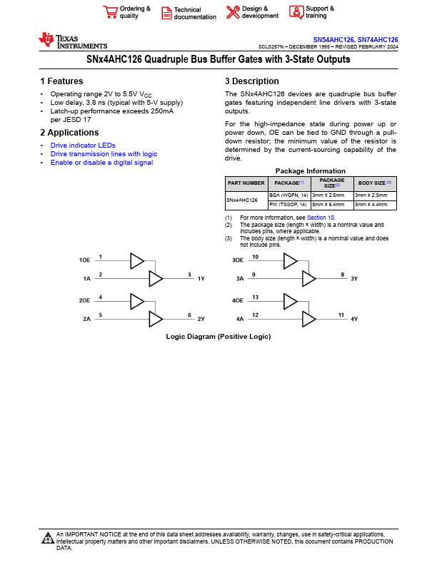
The SNx4AHC126 devices are quadruple bus buffer gates featuring independent line drivers with 3-state outputs.
For the high-impedance state during power up or power down, OE can be tied to GND through a pulldown resistor; the minimum value of the resistor is determined by the current-sourcing capability of the drive.
Package Information
PART NUMBER PACKAGE(1)
PACKAGE SIZE(2)
SNx4AHC126
BQA (WQFN, 14) 3mm × 2.5mm PW (TSSOP, 14) 5mm × 6.4mm
BODY SIZE (3)
3mm × 2.5mm 5mm × 4.4mm
(1) For more information, see Section 10. (2) The package size (length × width) is a nominal value and includes pins, where applicable. (3) The body size (length × width) is a nominal value and does not include pins.
Logic Diagram (Positive Logic)
An IMPORTANT NOTICE at the end of this data sheet addresses availability, warranty, changes, use in safety-critical applications, intellectual property matters and other important disclaimers. UNLESS OTHERWISE NOTED, this document contains PRODUCTION DATA.
SN54AHC126, SN74AHC126
SCLS257N
- DECEMBER 1995
- REVISED FEBRUARY 2024...