SN74AHC1G32-Q1 Overview
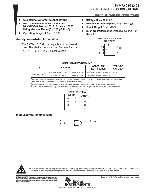
/ordering information The SN74AHC1G32 is a single 2-input positive-OR gate. The device performs the Boolean function Y + A ) B or Y + A B in positive logic. ‡ Package drawings, thermal data, and symbolization are available at http://.ti./packaging.