Datasheet4U Logo Datasheet4U.com

SN74AUC126 - QUADRUPLE BUS BUFFER GATE

Description

This quadruple bus buffer gate is designed for 0.8-V to 2.7-V VCC operation, but is designed specifically for 1.6-V to 1.95-V VCC operation.

The SN74AUC126 contains four independent line drivers with 3-state outputs.

Features

  • Optimized for 1.8-V Operation and Is 3.6-V I/O Tolerant to Support Mixed-Mode Signal Operation.
  • Ioff Supports Partial-Power-Down Mode Operation.
  • Sub 1-V Operable.
  • Max tpd of 2.1 ns at 1.8 V.
  • Low Power Consumption, 10-µA Max ICC.
  • ±8-mA Output Drive at 1.8 V.
  • Latch-Up Performance Exceeds 100 mA Per JESD 78, Class II.
  • ESD Protection Exceeds JESD 22.
  • 2000-V Human-Body Model (A114-A).
  • 200-V Machine Model (A115-.

📥 Download Datasheet

Datasheet preview – SN74AUC126

Datasheet Details

Part number SN74AUC126
Manufacturer Texas Instruments
File Size 816.78 KB
Description QUADRUPLE BUS BUFFER GATE
Datasheet download datasheet SN74AUC126 Datasheet
Additional preview pages of the SN74AUC126 datasheet.
Other Datasheets by Texas Instruments

Full PDF Text Transcription

Click to expand full text
www.ti.com FEATURES • Optimized for 1.8-V Operation and Is 3.6-V I/O Tolerant to Support Mixed-Mode Signal Operation • Ioff Supports Partial-Power-Down Mode Operation • Sub 1-V Operable • Max tpd of 2.1 ns at 1.8 V • Low Power Consumption, 10-µA Max ICC • ±8-mA Output Drive at 1.8 V • Latch-Up Performance Exceeds 100 mA Per JESD 78, Class II • ESD Protection Exceeds JESD 22 – 2000-V Human-Body Model (A114-A) – 200-V Machine Model (A115-A) – 1500-V Charged-Device Model (C101) GND 3Y SN74AUC126 QUADRUPLE BUS BUFFER GATE WITH 3-STATE OUTPUTS SCES509 – NOVEMBER 2003 – REVISED DECEMBER 2005 
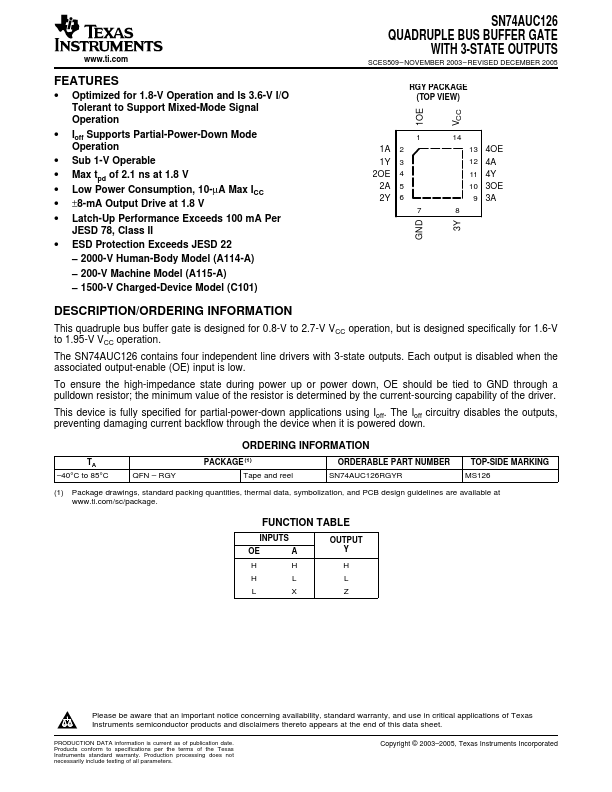
RGY PACKAGE (TOP VIEW) 1OE VCC 1 1A 2 1Y 3 2OE 4 2A 5 2Y 6 7 14 13 4OE 12 4A 11 4Y 10 3OE 9 3A 8 DESCRIPTION/ORDERING INFORMATION This quadruple bus buffer gate is designed for 0.8-V to 2.
Published: |