Datasheet4U.com
🌙
SN74CBT3125 Datasheet | Texas Instruments
Part:
SN74CBT3125
Description:
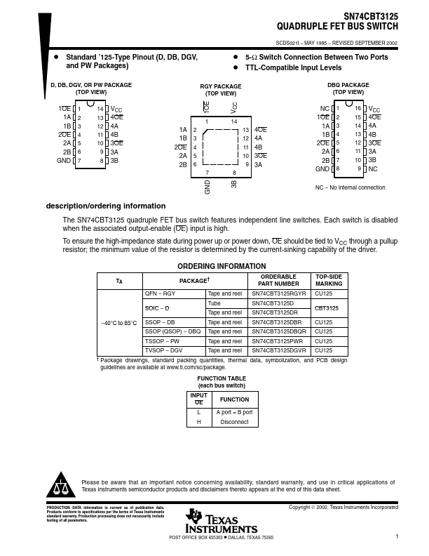
QUADRUPLE FET BUS SWITCH
Manufacturer:
Texas Instruments
Size:
1.36 MB
SN74CBT3125 Datasheet (PDF) Download
Related SN74CBT3125 Datasheets
SN74CBT3125D QUADRUPLE FET BUS SWITCH
SN74CBT3125C QUADRUPLE FET BUS SWITCH
SN74CBT3125CD QUADRUPLE FET BUS SWITCH
SN74CBT3126 QUADRUPLE FET BUS SWITCH
SN74CBT3126D QUADRUPLE FET BUS SWITCH
Texas Instruments
SN74CBT3125
Key Features
independent line switches. Each switch is disabled when the associated output-enable (OE) input is high
×
Close