SN74CBT3125D
description
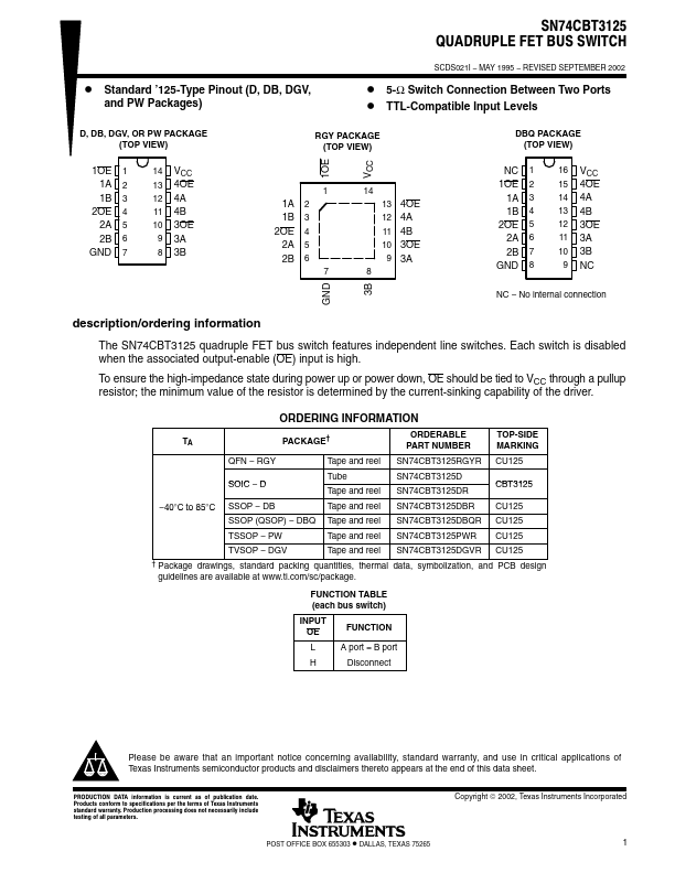
/ordering information
The SN74CBT3125 quadruple FET bus switch features independent line switches. Each switch is disabled when the associated output-enable (OE) input is high.
To ensure the high-impedance state during power up or power down, OE should be tied to VCC through a pullup resistor; the minimum value of the resistor is determined by the current-sinking capability of the driver.
ORDERING INFORMATION
PACKAGE†
ORDERABLE PART NUMBER
TOP-SIDE MARKING
- RGY
Tape and reel SN74CBT3125RGYR CU125
SOIC
- D
Tube Tape and reel
SN74CBT3125D SN74CBT3125DR
CBT3125
- 40°C to 85°C SSOP
- DB
Tape and reel
SSOP (QSOP)
- DBQ Tape and reel
SN74CBT3125DBR CU125 SN74CBT3125DBQR CU125
TSSOP
- PW
Tape and reel SN74CBT3125PWR CU125
TVSOP
- DGV
Tape and reel SN74CBT3125DGVR CU125
† Package drawings, standard packing quantities, thermal data, symbolization, and PCB design guidelines are available at .ti./sc/package.
FUNCTION TABLE (each bus switch)
INPUT...