Datasheet4U Logo Datasheet4U.com

SN74CBTD3306C - DUAL FET BUS SWITCH

Description

The SN74CBTD3306C is a high-speed TTL-compatible FET bus switch with low ON-state resistance (ron), allowing for minimal propagation delay.

Features

  • an integrated diode in series with VCC to provide level shifting for 5-V input down to 3.3-V output levels. Active Undershoot-Protection Circuitry on the A and B ports of the SN74CBTD3306C provides protection for undershoot up to.
  • 2 V by sensing an undershoot event and ensuring that the switch remains in the proper OFF state. The SN74CBTD3306C is organized as two 1-bit bus switches with separate output-enable (1OE, 2OE) inputs. It can be used as two 1-bit bus switches or as one 2-bit bus.

📥 Download Datasheet

Datasheet preview – SN74CBTD3306C

Datasheet Details

Part number SN74CBTD3306C
Manufacturer Texas Instruments
File Size 782.03 KB
Description DUAL FET BUS SWITCH
Datasheet download datasheet SN74CBTD3306C Datasheet
Additional preview pages of the SN74CBTD3306C datasheet.
Other Datasheets by Texas Instruments

Full PDF Text Transcription

Click to expand full text
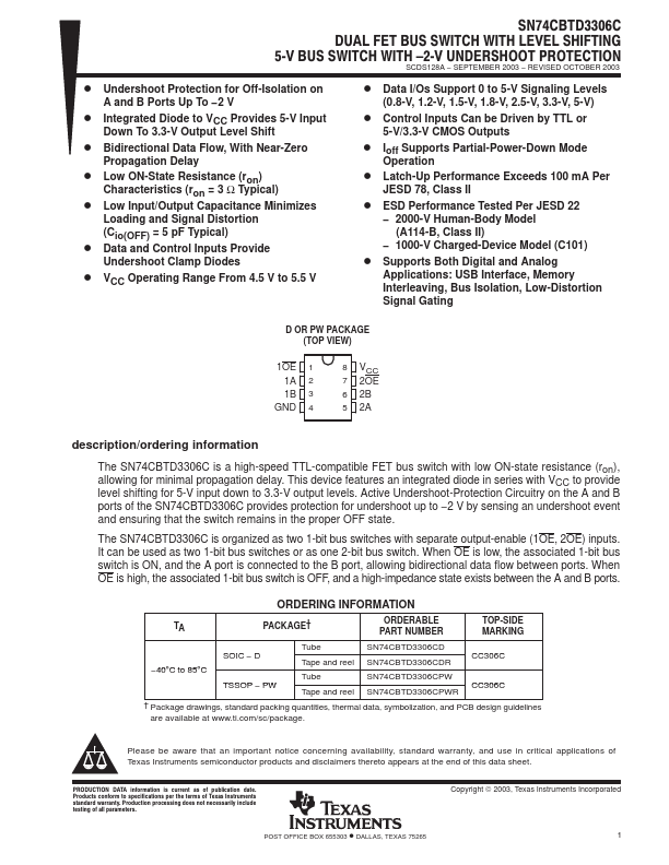
SN74CBTD3306C DUAL FET BUS SWITCH WITH LEVEL SHIFTING 5ĆV BUS SWITCH WITH ć2ĆV UNDERSHOOT PROTECTION SCDS128A − SEPTEMBER 2003 − REVISED OCTOBER 2003 D Undershoot Protection for Off-Isolation on A and B Ports Up To −2 V D Integrated Diode to VCC Provides 5-V Input Down To 3.3-V Output Level Shift D Bidirectional Data Flow, With Near-Zero Propagation Delay D Low ON-State Resistance (ron) Characteristics (ron = 3 Ω Typical) D Low Input/Output Capacitance Minimizes Loading and Signal Distortion (Cio(OFF) = 5 pF Typical) D Data and Control Inputs Provide Undershoot Clamp Diodes D VCC Operating Range From 4.5 V to 5.5 V D Data I/Os Support 0 to 5-V Signaling Levels (0.8-V, 1.2-V, 1.5-V, 1.8-V, 2.5-V, 3.3-V, 5-V) D Control Inputs Can be Driven by TTL or 5-V/3.
Published: |