SN74HCT02D
Features
- Operating voltage range of 4.5V to 5.5V
- Outputs can drive up to 10 LSTTL loads
- Low power consumption, 20-µA max ICC
- Typical tpd = 10ns
- ±4-m A output drive at 5V
- Low input current of 1µA max
- Inputs are TTL-Voltage patible
2 Description
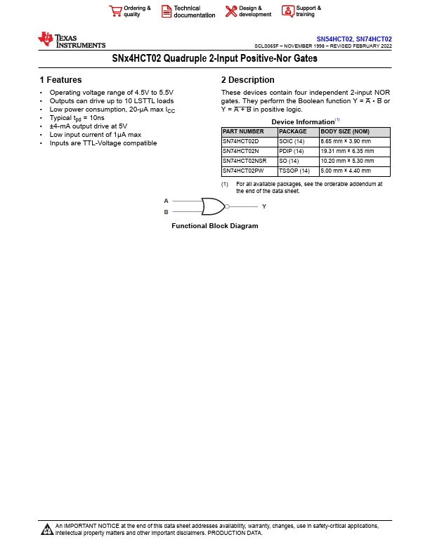
These devices contain four independent 2-input NOR gates. They perform the Boolean function Y = A
- B or Y = A + B in positive logic.
Device Information(1)
PART NUMBER
PACKAGE
BODY SIZE (NOM)
SOIC (14)
8.65 mm × 3.90 mm
SN74HCT02N
PDIP (14)
19.31 mm × 6.35 mm
SN74HCT02NSR SO (14)
10.20 mm × 5.30 mm
SN74HCT02PW
TSSOP (14) 5.00 mm × 4.40 mm
(1) For all available packages, see the orderable addendum at the end of the data sheet.
Functional Block Diagram
An IMPORTANT NOTICE at the end of this data sheet addresses availability, warranty, changes, use in safety-critical applications, intellectual property matters and other important disclaimers. PRODUCTION DATA.
SN54HCT02, SN74HCT02
SCLS065F
- NOVEMBER 1998
-...