SN75179A
description
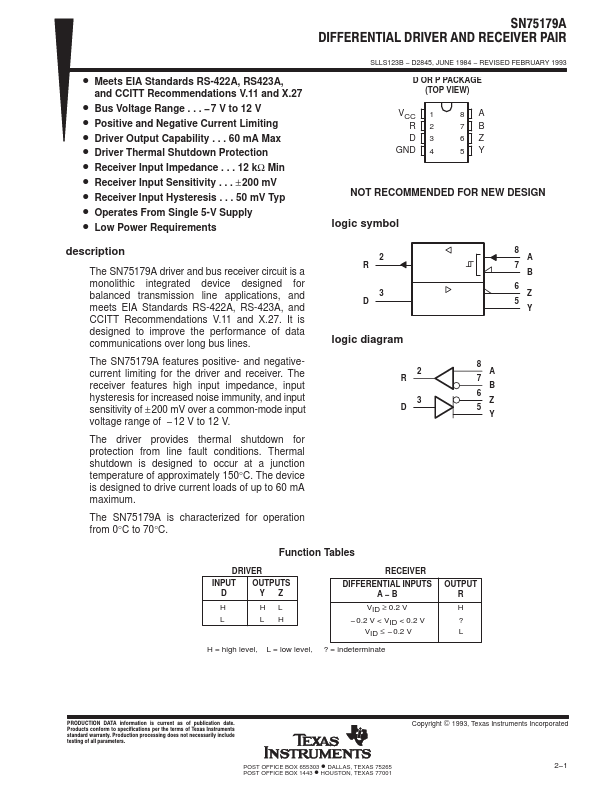
The SN75179A driver and bus receiver circuit is a monolithic integrated device designed for balanced transmission line applications, and meets EIA Standards RS-422A, RS-423A, and CCITT Remendations V.11 and X.27. It is designed to improve the performance of data munications over long bus lines.
The SN75179A features positive- and negativecurrent limiting for the driver and receiver. The receiver features high input impedance, input hysteresis for increased noise immunity, and input sensitivity of ± 200 m V over a mon-mode input voltage range of
- 12 V to 12 V.
The driver provides thermal shutdown for protection from line fault conditions. Thermal shutdown is designed to occur at a junction temperature of approximately 150°C. The device is designed to drive current loads of up to 60 m A maximum.
The SN75179A is characterized for operation from 0°C to 70°C.
2 R
3 D logic diagram
2 R
3 D
8 A
7 B
6 Z
5 Y
8 A
7 B
6 Z
5 Y
Function Tables
DRIVER
INPUT D
OUTPUTS YZ
H HL L...