SN75LBC175A Overview
Key Specifications
Package: PDIP
Mount Type: Through Hole
Pins: 16
Operating Voltage: 5 V
Description
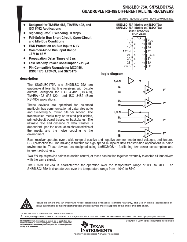
1,2EN The SN65LBC175A and SN75LBC175A are quadruple differential line receivers with 3-state 1A 1Y outputs, designed for TIA/EIA-485 (RS-485), 1B TIA/EIA-422 (RS-422), and ISO 8482 (Euro RS-485) applications. 2A These devices are optimized for balanced 2B 2Y multipoint bus communication at data rates up to and exceeding 50 million bits per second.
Key Features
- ESD protection to 6 kV, making it suitable for high-speed multipoint data transmission applications in harsh environments
- These devices are designed using LinBiCMOSt, facilitating low power consumption and inherent robustness
- Two EN inputs provide pair-wise enable control, or these can be tied together externally to enable all four drivers with the same signal
- The SN75LBC175A is characterized for operation over the temperature range of 0°C to 70°C
- The SN65LBC175A is characterized over the