SNJ54HC541J Description
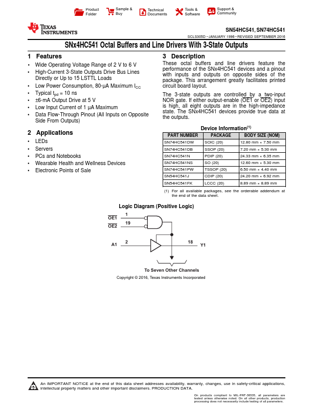
These octal buffers and line drivers.
SNJ54HC541J Key Features
- 1 Wide Operating Voltage Range of 2 V to 6 V
- High-Current 3-State Outputs Drive Bus Lines
- Low Power Consumption, 80-µA Maximum ICC
- Typical tpd = 10 ns
- ±6-mA Output Drive at 5 V
- Low Input Current of 1 µA Maximum
- Data Flow-Through Pinout (All Inputs on Opposite