APPLICATIONS
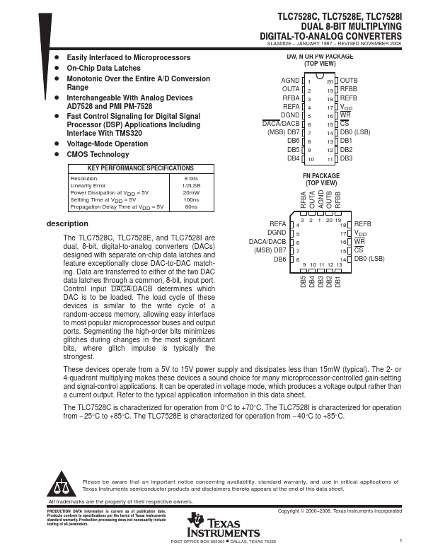
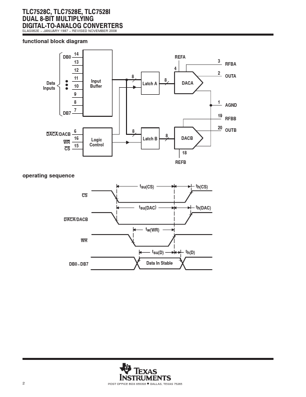
Including Interface With TMS320 D Voltage-Mode Operation D CMOS Technology KEY PERFORMANCE SPECIFICATIONS Resolution Linearity Error Power Dissipation at VDD = 5V Settling Time at VDD = 5V Propagation Delay Time at VDD = 5V 8 bits 1/2LSB 20mW 100ns 80ns RFBA OUTA DW, N OR PW PACKAGE (TOP VIEW) AGND 1 OUTA 2 RFBA 3 REFA 4 DGND 5 DACA/DACB 6 (MSB) DB7 7 DB6 8 DB5 9 DB4 10 20 OUTB 19 RFBB 18 REFB 17 VDD 16 WR 15 CS 14 DB0 (LSB) 13 DB1 12 DB2 11 DB3 FN PACKAGE (TOP VIEW) AGND OUTB RFBB description Data are transferred to either of the two DAC data latches through a common, 8-bit, input port. Control input DACA/DACB determines which DAC is to be loaded. Segmenting the high-order bits minimizes glitches during changes in the most significant bits, where glitch impulse is typically the strongest. DB5 DB4 REFA DGND DACA/DACB (MSB) DB7 DB6 3 2 1 20 19 4 18 5 17 6 16 7 15 8 14 9 10 11 12 13 REFB VDD WR CS DB0 (LSB) DB3 DB2 DB1 These devices operate from a 5V to 15V power supply and dissipates less than 15mW (typical). Texas Instruments