TPS22925 Key Features
- 1 Input Voltage Range: 0.65 V to 3.6 V
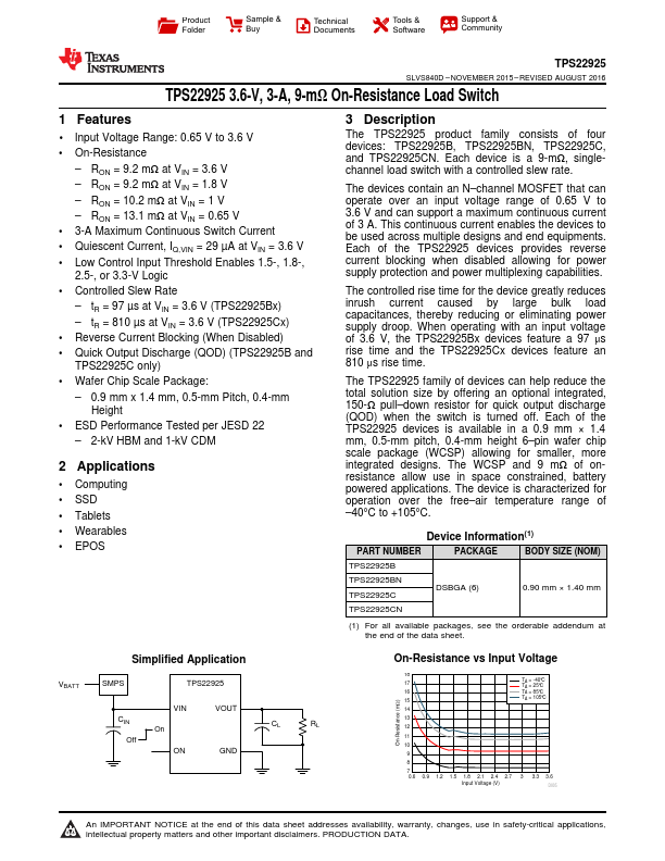
- On-Resistance
- RON = 9.2 mΩ at VIN = 3.6 V
- RON = 9.2 mΩ at VIN = 1.8 V
- RON = 10.2 mΩ at VIN = 1 V
- RON = 13.1 mΩ at VIN = 0.65 V
- 3-A Maximum Continuous Switch Current
- Quiescent Current, IQ,VIN = 29 µA at VIN = 3.6 V
- Low Control Input Threshold Enables 1.5-, 1.8-, 2.5-, or 3.3-V Logic
- Controlled Slew Rate