www.ti.com
TPS63900
SLVSET3D – MARCH 2020 – REVISED OCTTOPBSE6R32900200
SLVSET3D – MARCH 2020 – REVISED OCTOBER 2020
TPS63900 1.8-V to 5.5-V, 75-nA IQ Buck-boost Converter with Input Current Limit and
DVS
1 Features
• Input voltage range: 1.8 V to 5.5 V
• Output voltage range: 1.8 V to 5 V (100-mV steps)
– Programmable with external resistors
– SEL pin to toggle between two output voltage
presets
• > 400-mA output current for VI ≥ 2.0 V, VO = 3.3 V
(typical 1.45-A peak switching current limit)
– Stackable: parallel multiple devices for higher
output current
• > 90% Efficiency at 10-µA load current
– 75-nA quiescent current
– 60-nA shutdown current
• Single-mode operation
– Eliminates mode transitions between buck,
buck-boost and boost operation
– Low output ripple
– Excellent transient performance
• Safety and robust operation features
– Integrated soft start
– Programmable input current limit with eight
settings (1 mA to 100 mA and unlimited)
– Output short-circuit and overtemperature
protection
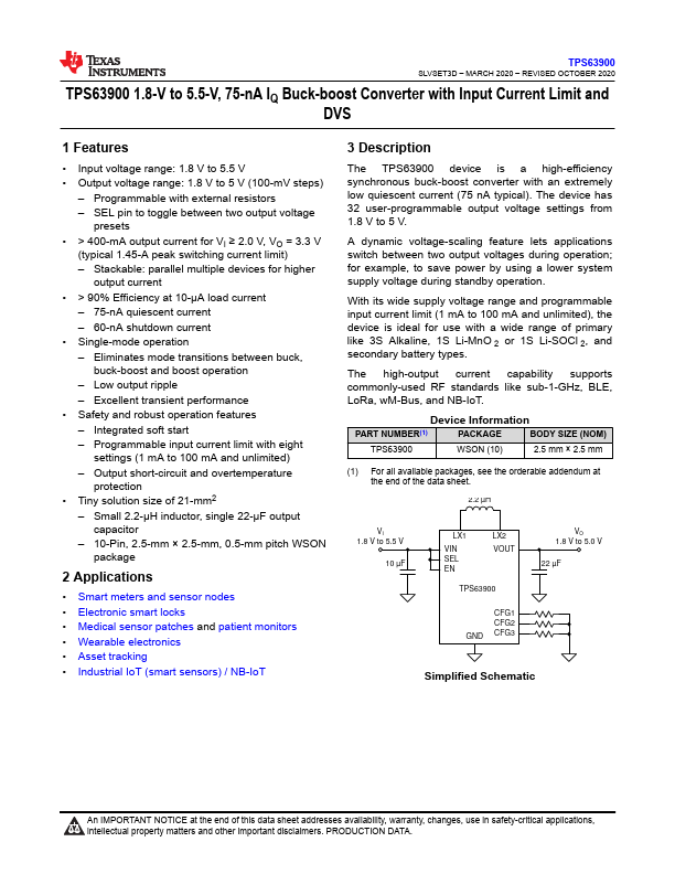
• Tiny solution size of 21-mm2
– Small 2.2-µH inductor, single 22-µF output
capacitor
– 10-Pin, 2.5-mm × 2.5-mm, 0.5-mm pitch WSON
package
2 Applications
• Smart meters and sensor nodes
• Electronic smart locks
• Medical sensor patches and patient monitors
• Wearable electronics
• Asset tracking
• Industrial IoT (smart sensors) / NB-IoT
3 Description
The TPS63900 device is a high-efficiency
synchronous buck-boost converter with an extremely
low quiescent current (75 nA typical). The device has
32 user-programmable output voltage settings from
1.8 V to 5 V.
A dynamic voltage-scaling feature lets applications
switch between two output voltages during operation;
for example, to save power by using a lower system
supply voltage during standby operation.
With its wide supply voltage range and programmable
input current limit (1 mA to 100 mA and unlimited), the
device is ideal for use with a wide range of primary
like 3S Alkaline, 1S Li-MnO 2 or 1S Li-SOCl 2, and
secondary battery types.
The high-output current capability supports
commonly-used RF standards like sub-1-GHz, BLE,
LoRa, wM-Bus, and NB-IoT.
Device Information
PART NUMBER(1)
PACKAGE
BODY SIZE (NOM)
TPS63900
WSON (10)
2.5 mm × 2.5 mm
(1) For all available packages, see the orderable addendum at
the end of the data sheet.
2.2 µH
VI
1.8 V to 5.5 V
10 µF
LX1
VIN
SEL
EN
LX2
VOUT
TPS63900
GND
CFG1
CFG2
CFG3
VO
1.8 V to 5.0 V
22 µF
Simplified Schematic
An IMPORTANT NOTICE at the end of this data sheet addresses availability, warranty, changes, use in safety-critical applications,
Copyrighint t©el2le0c2t0uTael xparsoIpnesrtrtuymmeanttsteIrnscoarnpdoraottehder important disclaimers. PRODUCTION DATA.
Submit Document Feedback
1
Product Folder Links: TPS63900