TS5A1066 Description
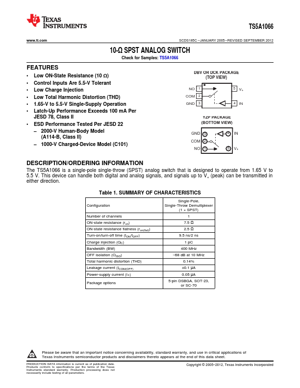
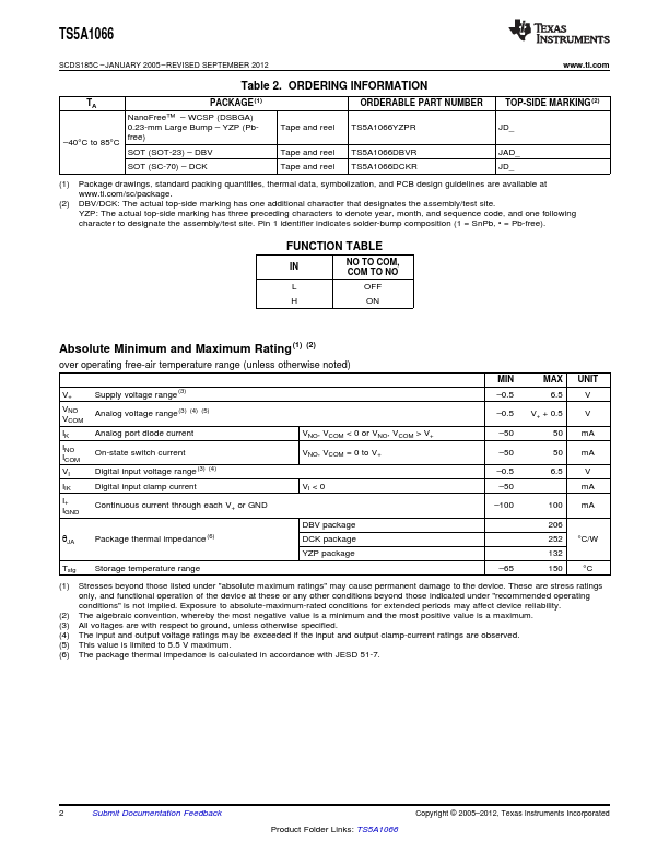
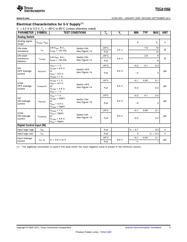
/ORDERING INFORMATION The TS5A1066 is a single-pole single-throw (SPST) analog switch that is designed to operate from 1.65 V to 5.5 V. This device can handle both digital and analog signals, and signals up to V+ (peak) can be transmitted in either direction. PRODUCTION DATA information is current as of publication date.
TS5A1066 Key Features
- Low ON-State Resistance (10 Ω)
- Control Inputs Are 5.5-V Tolerant
- Low Charge Injection
- Low Total Harmonic Distortion (THD)
- 1.65-V to 5.5-V Single-Supply Operation
- ESD Performance Tested Per JESD 22
- 2000-V Human-Body Model (A114-B, Class II)
- 1000-V Charged-Device Model (C101)