TS5A9411
Description
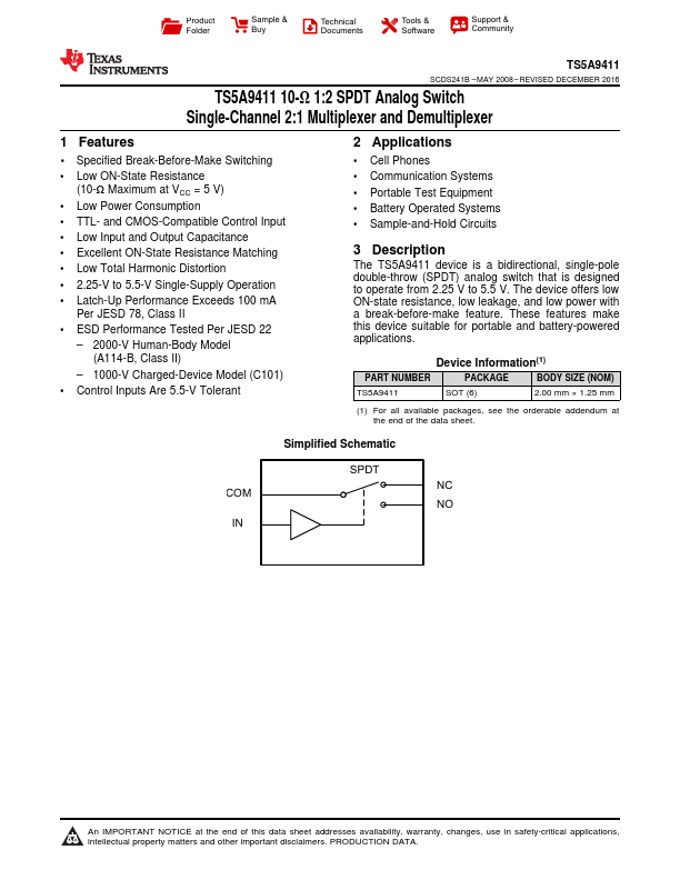
The TS5A9411 device is a bidirectional, single-pole double-throw (SPDT) analog switch that is designed to operate from 2.25 V to 5.5 V.
Key Features
- 1 Specified Break-Before-Make Switching
- Low ON-State Resistance (10-Ω Maximum at VCC = 5 V)
- Low Power Consumption
- Low Input and Output Capacitance
- Excellent ON-State Resistance Matching
- Low Total Harmonic Distortion
- 2.25-V to 5.5-V Single-Supply Operation
- Latch-Up Performance Exceeds 100 mA Per JESD 78, Class II
- ESD Performance Tested Per JESD 22
- 2000-V Human-Body Model (A114-B, Class II)