UCC27201A
Description
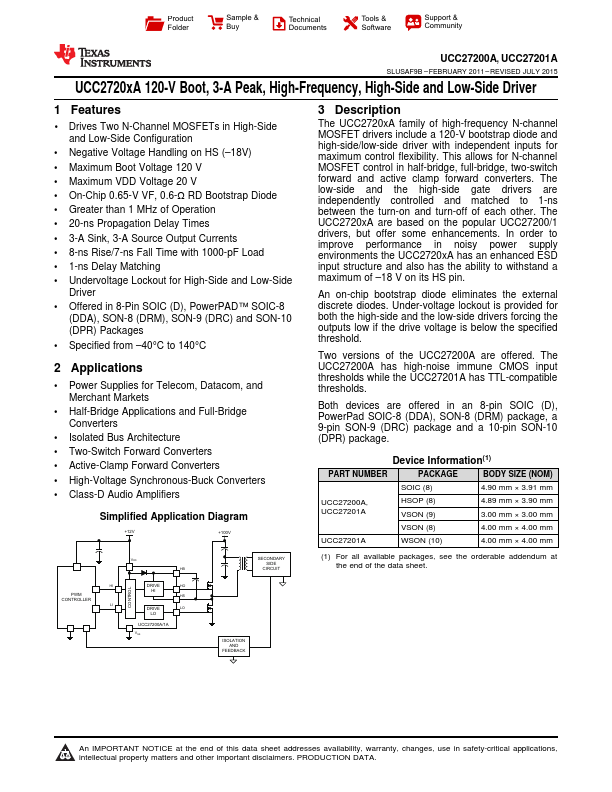
The UCC2720xA family of high-frequency N-channel MOSFET drivers include a 120-V bootstrap diode and high-side/low-side driver with independent inputs for maximum control flexibility. This allows for N-channel MOSFET control in half-bridge, full-bridge, two-switch forward and active clamp forward converters.
Key Features
- 1 Drives Two N-Channel MOSFETs in High-Side and Low-Side Configuration
- Negative Voltage Handling on HS (–18V)
- Maximum Boot Voltage 120 V
- Maximum VDD Voltage 20 V
- On-Chip 0.65-V VF, 0.6-Ω RD Bootstrap Diode
- Greater than 1 MHz of Operation
- 20-ns Propagation Delay Times
- 3-A Sink, 3-A Source Output Currents
- 8-ns Rise/7-ns Fall Time with 1000-pF Load
- 1-ns Delay Matching