UCC27423
UCC27423 is Dual 4-A High Speed Low-Side MOSFET Drivers manufactured by Texas Instruments.
UCC27423, UCC27424, UCC27425
SLUS545F
- NOVEMBER 2002
- REVISED NOVEMBER 2023
UCC2742x Dual 4-A High Speed Low-Side MOSFET Drivers With Enable
1 Features
- Industry-Standard Pin-Out
- Enable Functions for Each Driver
- High Current Drive Capability of ±4 A
- Unique Bi Polar and CMOS True Drive Output
Stage Provides High Current at MOSFET Miller Thresholds
- TTL/CMOS patible Inputs Independent of Supply Voltage
- 20-ns Typical Rise and 15-ns Typical Fall Times with 1.8-n F Load
- Typical Propagation Delay Times of 25 ns with Input Falling and 35 ns with Input Rising
- 4-V to 15-V Supply Voltage
- Dual Outputs Can Be Paralleled for Higher Drive Current
- Available in Thermally Enhanced MSOP Power PAD™ Package
- Rated From
- 40°C to 125°C
2 Applications
- Switch Mode Power Supplies
- DC/DC Converters
- Motor Controllers
- Line Drivers
- Class D Switching Amplifiers
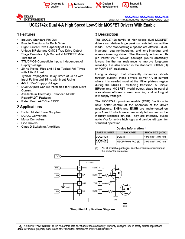
ENBB
3 Description
The UCC2742x family of high-speed dual MOSFET drivers can deliver large peak currents into capacitive loads. Three standard logic options are offered
- dualinverting, dual-noninverting, and one-inverting and one-noninverting driver. The thermally enhanced 8pin Power PAD™ MSOP package (DGN) drastically lowers the thermal resistance to improve long-term reliability. It is also offered in the standard SOIC-8 (D) or PDIP-8 (P) packages.
Using a design that inherently minimizes shootthrough current, these drivers deliver 4A of current where it is needed most at the Miller plateau region during the MOSFET switching transition. A unique Bi Polar and MOSFET hybrid output stage in parallel also allows efficient current sourcing and sinking at low supply...