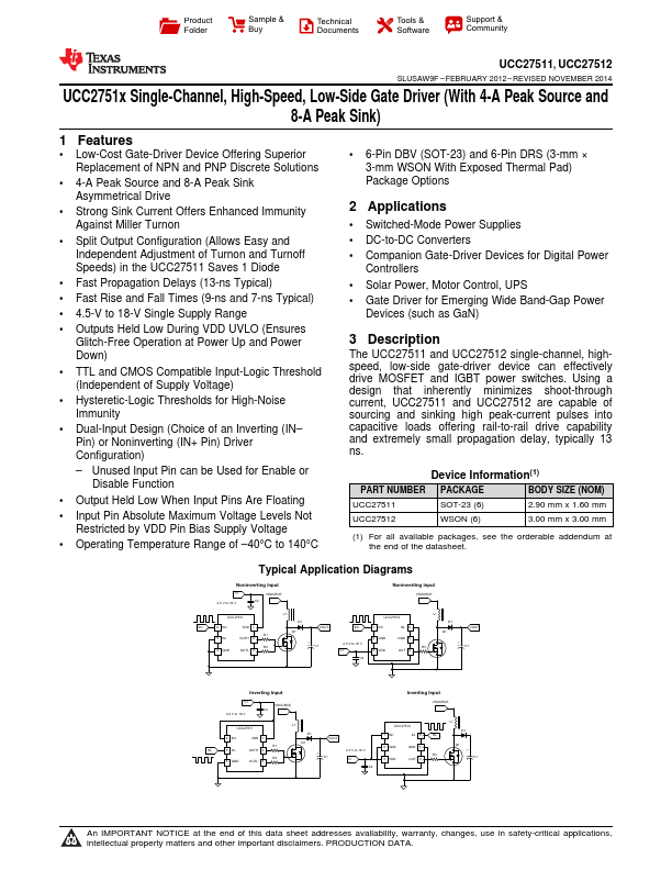
UCC27511, UCC27512
SLUSAW9F – FEBRUARY 2012 – REVISED NOVEMBER 2014
www.ti.com
Table of Contents
1 Features .................................................................. 1
2 Applications ........................................................... 1
3 Description ............................................................. 1
4 Revision History..................................................... 2
5 Description (Continued) ........................................ 4
6 UCC2751x Product Family .................................... 4
7 Pin Configuration and Functions ......................... 5
8 Specifications......................................................... 7
8.1 Absolute Maximum Ratings ...................................... 7
8.2 Handling Ratings....................................................... 7
8.3 Recommended Operating Conditions....................... 7
8.4 Thermal Information .................................................. 8
8.5 Electrical Characteristics........................................... 9
8.6 Switching Characteristics ........................................ 10
8.7 Typical Characteristics ............................................ 12
9 Detailed Description ............................................ 15
9.1 Overview ................................................................. 15
9.2 Functional Block Diagram ....................................... 15
9.3 Feature Description................................................. 16
9.4 Device Functional Modes........................................ 21
10 Application and Implementation........................ 22
10.1 Application Information.......................................... 22
10.2 Typical Application ................................................ 22
11 Power Supply Recommendations ..................... 27
12 Layout................................................................... 27
12.1 Layout Guidelines ................................................. 27
12.2 Layout Example .................................................... 28
13 Device and Documentation Support ................. 29
13.1 Related Links ........................................................ 29
13.2 Trademarks ........................................................... 29
13.3 Electrostatic Discharge Caution ............................ 29
13.4 Glossary ................................................................ 29
14 Mechanical, Packaging, and Orderable
Information ........................................................... 29
4 Revision History
NOTE: Page numbers for previous revisions may differ from page numbers in the current version.
Changes from Revision E (December 2013) to Revision F
Page
• Added Pin Configuration and Functions section, Handling Rating table, Feature Description section, Device
Functional Modes, Application and Implementation section, Power Supply Recommendations section, Layout
section, Device and Documentation Support section, and Mechanical, Packaging, and Orderable Information
section ................................................................................................................................................................................... 1
Changes from Revision D (May 2013) to Revision E
Page
• Changed OUTL in the ABS Max Ratings table to show DC and Repetitive pulse values ..................................................... 7
Changes from Revision C (June 2012) to Revision D
Page
• Added 0.05 to PSW equation in the Power Dissipation section. ........................................................................................... 26
Changes from Revision B (March, 2012) to Revision C
Page
• Added UCC27512 device throughout. ................................................................................................................................... 1
• Added 6-Pin DRS package feature. ....................................................................................................................................... 1
• Added DRS pinout for the UCC27512.................................................................................................................................... 5
• Added UCC27512 TERMINAL FUNCTIONS table. ............................................................................................................... 6
• Added OUT voltage ab max ratings for the UCC27512. ........................................................................................................ 7
• Added (1) ................................................................................................................................................................................. 7
• Changed ESD ratings of Human Body Model, HBM from 2000 V to 4000 V. ....................................................................... 7
• Changed ESD ratings of Charged Device Model, CDM SOT-23 from 500 V to 1000 V........................................................ 7
• Added UCC27512 Thermal Information. ................................................................................................................................ 8
• Added power dissipation conditions note to Thermal Information section. ............................................................................ 8
• Added UCC27512 Functional Block Diagram. ..................................................................................................................... 16
(1) Values are verified by characterization on bench.
2 Submit Documentation Feedback
Copyright © 2012–2014, Texas Instruments Incorporated
Product Folder Links: UCC27511 UCC27512