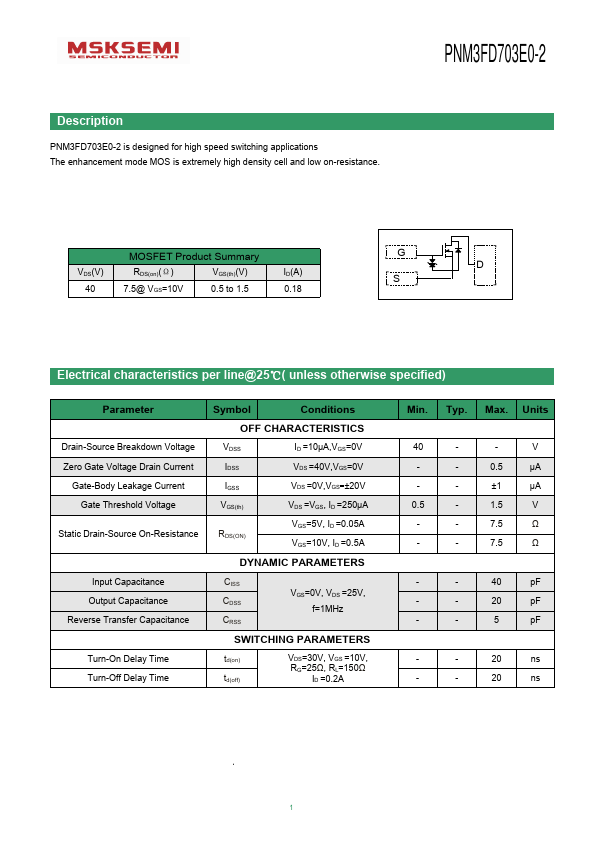
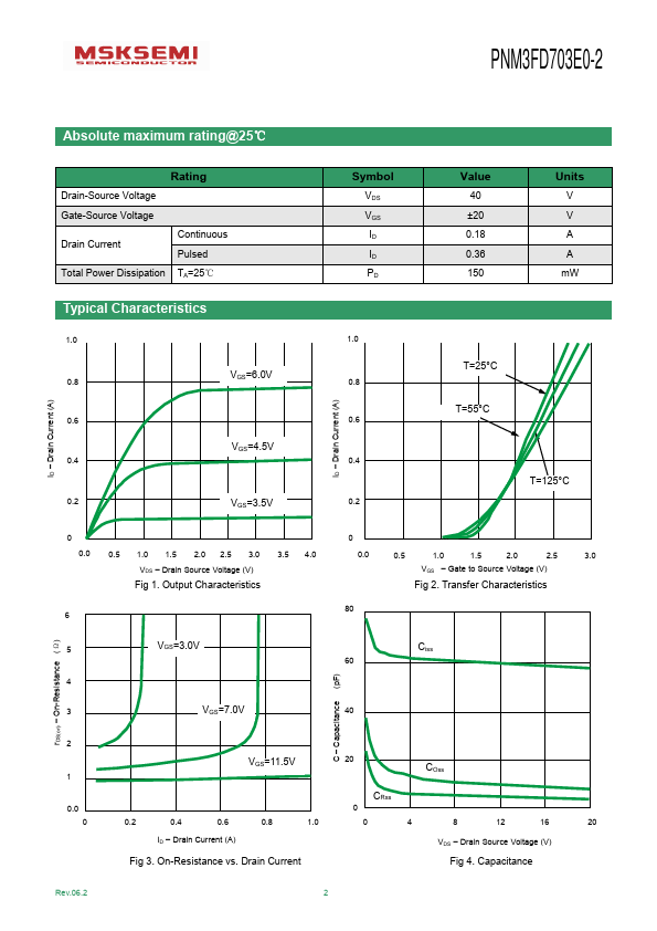
Click to expand full text
PNM3FD703E0-2
N-Channel MOSFET
Description
PNM3FD703E0-2 is designed for high speed switching applications The enhancement mode MOS is extremely high density cell and low on-resistance.
VDS(V) 40
MOSFET Product Summary
RDS(on)(Ω)
VGS(th)(V)
7.5@ VGS=10V
0.5 to 1.5
ID(A) 0.18
G D
S
Electrical characteristics per line@25℃( unless otherwise specified)
Parameter
Drain-Source Breakdown Voltage Zero Gate Voltage Drain Current
Gate-Body Leakage Current Gate Threshold Voltage
Static Drain-Source On-Resistance
Input Capacitance Output Capacitance Reverse Transfer Capacitance
Turn-On Delay Time Turn-Off Delay Time
Symbol
Conditions
OFF CHARACTERISTICS
VDSS
ID =10μA,VGS=0V
IDSS
VDS =40V,VGS=0V
IGSS
VDS =0V,VGS=±20V
VGS(th)
VDS =VGS, ID =250μA
RDS(ON)
VGS=5V, ID =0.