
74ALVC14PW Overview
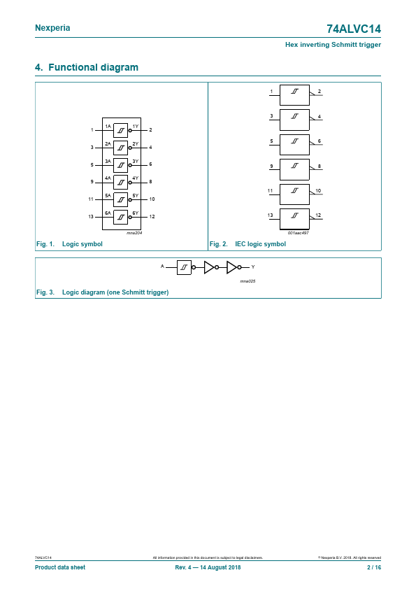
The 74ALVC14 is a high-performance, low-power, low-voltage, Si-gate CMOS device and superior to most advanced CMOS patible TTL families. The 74ALVC14 provides six inverting buffers with Schmitt-trigger action. It is capable of transforming slowly changing input signals into sharply defined, jitter-free output signals.
74ALVC14PW Key Features
- Wide supply voltage range from 1.65 V to 3.6 V
- 3.6 V tolerant inputs/outputs
- CMOS low power consumption
- Direct interface with TTL levels (2.7 V to 3.6 V)
- Power-down mode
- Unlimited input rise and fall times
- Latch-up performance exceeds 250 mA
- plies with JEDEC standard
- JESD8-7 (1.65 V to 1.95 V)
- JESD8-5 (2.3 V to 2.7 V)