74ALVC16836ADGG Overview
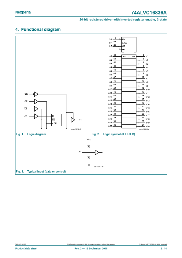
The 74ALVC16836A is a 20-bit universal bus driver. Data flow is controlled by active low output enable (OE), active low latch enable (LE) and clock inputs (CP). When LE is LOW, the A to Y data flow is transparent.
74ALVC16836ADGG Key Features
- Wide supply voltage range from 1.2 V to 3.6 V
- CMOS low-power consumption
- Direct interface with TTL levels
- Current drive ± 24 mA at 3.0 V
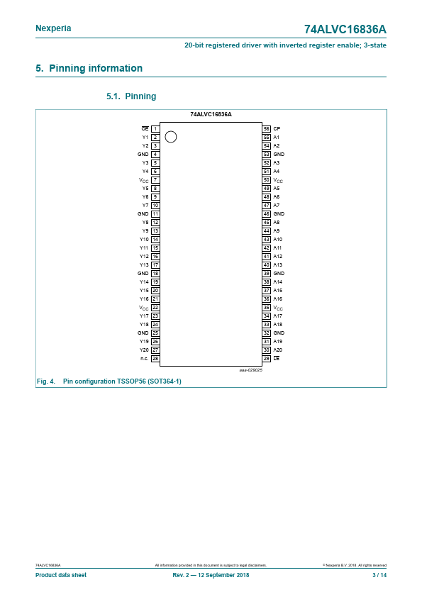
- MULTIBYTE flow-through standard pin-out architecture
- Low inductance multiple VCC and GND pins for minimum noise and ground bounce
- Output drive capability 50 Ω transmission lines at 85°C
- Input diodes to acmodate strong drivers
- plies with JEDEC standard no. 8-1A
- plies with JEDEC standards