Datasheet Summary
74HC107; 74HCT107
Dual JK flip-flop with reset; negative-edge trigger
Rev. 7
- 20 February 2024
Product data sheet
1. General description
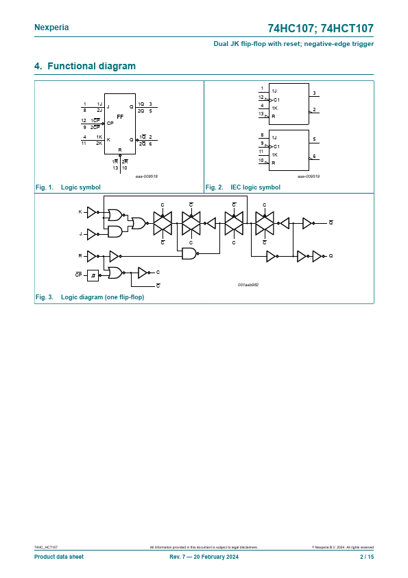
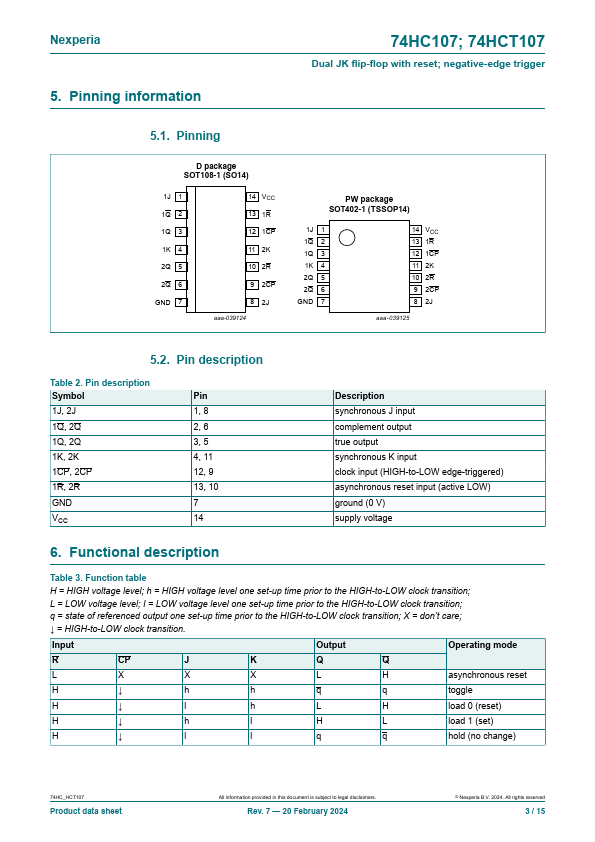
The 74HC107; 74HCT107 is a dual negative edge triggered JK flip-flop featuring individual J and K inputs, clock (CP) and reset (R) inputs and plementary Q and Q outputs. The reset is an asynchronous active LOW input and operates independently of the clock input. The J and K inputs control the state changes of the flip-flops as described in the mode select function table. The J and K inputs must be stable one set-up time prior to the HIGH-to-LOW clock transition for predictable operation. Inputs include clamp diodes that enable the use of current...