Datasheet4U Logo Datasheet4U.com

74HC194D - 4-bit bidirectional universal shift register

Download the 74HC194D datasheet PDF. This datasheet also covers the 74HC194 variant, as both devices belong to the same 4-bit bidirectional universal shift register family and are provided as variant models within a single manufacturer datasheet.

Description

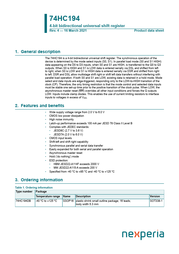
The 74HC194 is a 4-bit bidirectional universal shift register.

The synchronous operation of the device is determined by the mode select inputs (S0, S1).

In parallel load mode (S0 and S1 HIGH) data appearing on the D0 to D3 inputs, when S0 and S1 are HIGH, is transferred to the Q0 to Q3 outputs.

Features

  • Wide supply voltage range from 2.0 V to 6.0 V.
  • CMOS low power dissipation.
  • High noise immunity.
  • Latch-up performance exceeds 100 mA per JESD 78 Class II Level B.
  • Complies with JEDEC standards:.
  • JESD8C (2.7 V to 3.6 V).
  • JESD7A (2.0 V to 6.0 V).
  • CMOS input levels.
  • Shift-left and shift right capability.
  • Synchronous parallel and serial data transfer.
  • Easily expanded for both serial and parallel operat.

📥 Download Datasheet

Note: The manufacturer provides a single datasheet file (74HC194-nexperia.pdf) that lists specifications for multiple related part numbers.

Datasheet Details

Part number 74HC194D
Manufacturer Nexperia
File Size 236.02 KB
Description 4-bit bidirectional universal shift register
Datasheet download datasheet 74HC194D Datasheet

Full PDF Text Transcription (Reference)

The following content is an automatically extracted verbatim text from the original manufacturer datasheet and is provided for reference purposes only.

View original datasheet text
74HC194 4-bit bidirectional universal shift register Rev. 4 — 16 March 2021 Product data sheet 1. General description The 74HC194 is a 4-bit bidirectional universal shift register. The synchronous operation of the device is determined by the mode select inputs (S0, S1). In parallel load mode (S0 and S1 HIGH) data appearing on the D0 to D3 inputs, when S0 and S1 are HIGH, is transferred to the Q0 to Q3 outputs. When S0 is HIGH and S1 is LOW data is entered serially via DSL and shifted from left to right; when S0 is LOW and S1 is HIGH data is entered serially via DSR and shifted from right to left. DSR and DSL allow multistage shift right or shift left data transfers without interfering with parallel load operation. If both S0 and S1 are LOW, existing data is retained in a hold mode.
Published: |