74HC2G125DC Datasheet Text
74HC2G125; 74HCT2G125
Dual buffer/line driver; 3-state
Rev. 6
- 1 November 2018
Product data sheet
1. General description
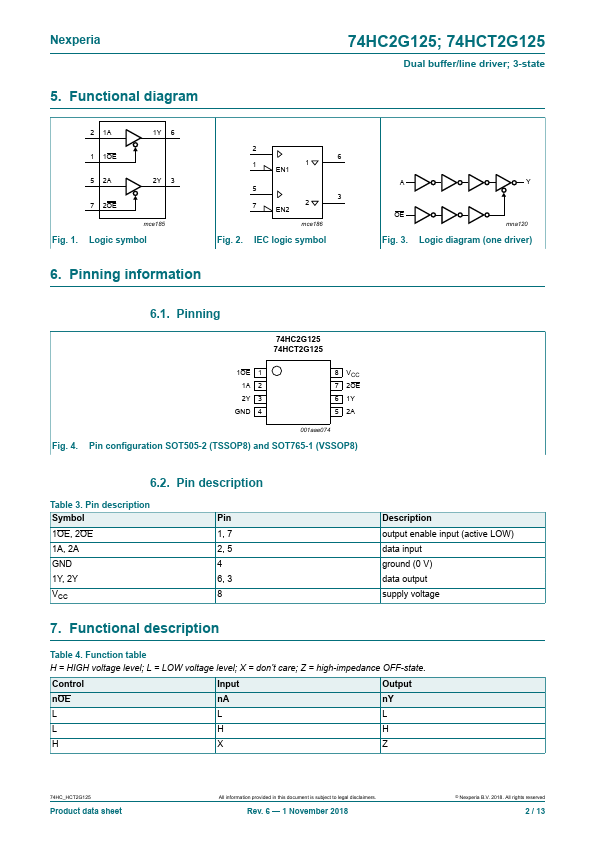
The 74HC2G125; 74HC2G125 are dual buffer/line drivers with 3-state outputs controlled by the output enable inputs (nOE). Inputs include clamp diodes which enable the use of current limiting resistors to interface inputs to voltages in excess of VCC.
2. Features and benefits
- Wide supply voltage range from 2.0 V to 6.0 V
- Input levels:
- For 74HC2G125: CMOS level
- For 74HCT2G125: TTL level
- Symmetrical output impedance
- High noise immunity
- Low power dissipation
- Balanced propagation delays
- ESD protection:
- HBM JESD22-A114F exceeds 2 000 V
- MM JESD22-A115-A exceeds 200 V
- Multiple package options
- Specified from -40 °C to +85 °C and -40 °C to +125 °C
3. Ordering information
Table 1. Ordering information
Type number
Package
Temperature range Name
74HC2G125DP -40 °C to +125 °C TSSOP8
74HCT2G125DP
74HC2G125DC -40 °C to +125 °C VSSOP8
74HCT2G125DC...