74HC3G34-Q100 Description
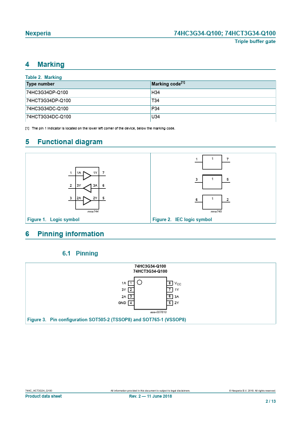
74HCT3G34-Q100 is a triple buffer. Inputs include clamp diodes. This enables the use of current limiting resistors to interface inputs to voltages in excess of VCC.
74HC3G34-Q100 Key Features
- Automotive product qualification in accordance with AEC-Q100 (Grade 1)
- Specified from -40 °C to +85 °C and from -40 °C to +125 °C
- Wide supply voltage range from 2.0 V to 6.0 V
- Input levels
- For 74HC3G34-Q100: CMOS level
- For 74HCT3G34-Q100: TTL level
- plies with JEDEC standard no. 7 A
- Symmetrical output impedance
- High noise immunity
- Low-power dissipation
74HC3G34-Q100 Applications
- Automotive product qualification in accordance with AEC-Q100 (Grade 1)
- Specified from -40 °C to +85 °C and from -40 °C to +125 °C
- Wide supply voltage range from 2.0 V to 6.0 V