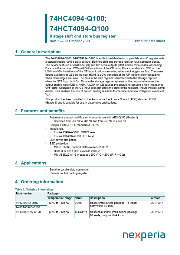
74HCT4094-Q100 Description
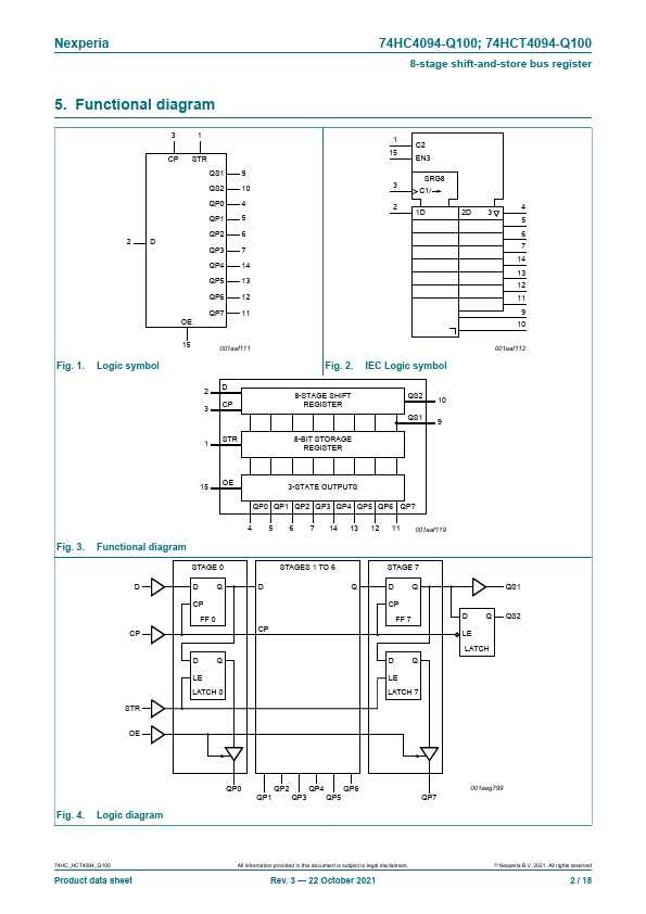
74HCT4094-Q100 is an 8-bit serial-in/serial or parallel-out shift register with a storage register and 3-state outputs. Both the shift and storage register have separate clocks.
74HCT4094-Q100 Applications
- Automotive product qualification in accordance with AEC-Q100 (Grade 1)
- Specified from -40 °C to +85 °C and from -40 °C to +125 °C
- plies with JEDEC standard JESD7A