74LVC07A Description
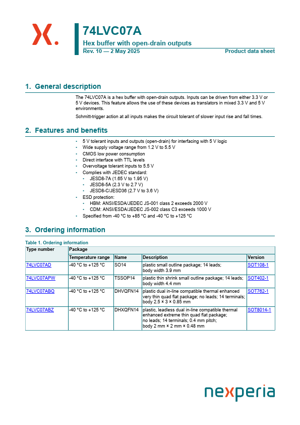
The 74LVC07A is a hex buffer with open-drain outputs. Inputs can be driven from either 3.3 V or 5 V devices.
74LVC07A Key Features
- 5 V tolerant inputs and outputs (open-drain) for interfacing with 5 V logic
- Wide supply voltage range from 1.2 V to 5.5 V
- CMOS low power consumption
- Direct interface with TTL levels
- Overvoltage tolerant inputs to 5.5 V
- plies with JEDEC standard
- JESD8-7A (1.65 V to 1.95 V)
- JESD8-5A (2.3 V to 2.7 V)
- JESD8-C/JESD36 (2.7 V to 3.6 V)
- ESD protection