74LVC4066-Q100 Description
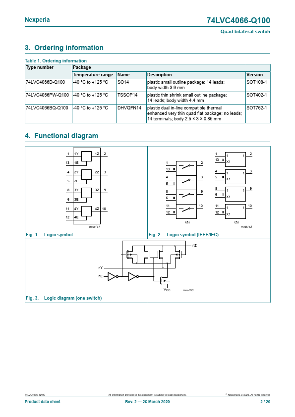
The 74LVC4066-Q100 is a high-speed Si-gate CMOS device. The 74LVC4066-Q100 provides four single pole, single-throw analog switch functions. Each switch has two input/output terminals (nY and nZ) and an active HIGH enable input (nE).
74LVC4066-Q100 Key Features
- Automotive product qualification in accordance with AEC-Q100 (Grade 1)
- Specified from -40 °C to +85 °C and from -40 °C to +125 °C
- Wide supply voltage range from 1.65 V to 5.5 V
- Very low ON resistance
- 7.5 Ω (typical) at VCC = 2.7 V
- 6.5 Ω (typical) at VCC = 3.3 V
- 6 Ω (typical) at VCC = 5 V
- Switch current capability of 32 mA
- High noise immunity
- CMOS low-power consumption
74LVC4066-Q100 Applications
- Automotive product qualification in accordance with AEC-Q100 (Grade 1)
- Specified from -40 °C to +85 °C and from -40 °C to +125 °C
- Wide supply voltage range from 1.65 V to 5.5 V