Datasheet4U Logo Datasheet4U.com

74LVC4066 - Quad bilateral switch

General Description

The 74LVC4066 is a high-speed Si-gate CMOS device.

The 74LVC4066 provides four single pole, single-throw analog switch functions.

Each switch has two input/output terminals (nY and nZ) and an active HIGH enable input (nE).

Key Features

  • Wide supply voltage range from 1.65 V to 5.5 V.
  • Very low ON resistance:.
  • 7.5 Ω (typical) at VCC = 2.7 V.
  • 6.5 Ω (typical) at VCC = 3.3 V.
  • 6 Ω (typical) at VCC = 5 V.
  • Switch current capability of 32 mA.
  • High noise immunity.
  • CMOS low-power consumption.
  • Direct interface TTL-levels.
  • Latch-up performance exceeds 250 mA.
  • ESD protection:.
  • HBM JESD22-A114F exceeds 2000 V.
  • MM JESD22-A115-A.

📥 Download Datasheet

Full PDF Text Transcription (Reference)

The following content is an automatically extracted verbatim text from the original manufacturer datasheet and is provided for reference purposes only.

View original datasheet text
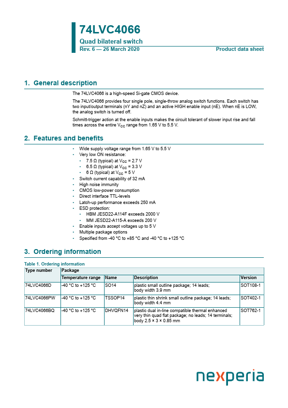
74LVC4066 Quad bilateral switch Rev. 6 — 26 March 2020 Product data sheet 1. General description The 74LVC4066 is a high-speed Si-gate CMOS device. The 74LVC4066 provides four single pole, single-throw analog switch functions. Each switch has two input/output terminals (nY and nZ) and an active HIGH enable input (nE). When nE is LOW, the analog switch is turned off. Schmitt-trigger action at the enable inputs makes the circuit tolerant of slower input rise and fall times across the entire VCC range from 1.65 V to 5.5 V. 2. Features and benefits • Wide supply voltage range from 1.65 V to 5.5 V • Very low ON resistance: • 7.5 Ω (typical) at VCC = 2.7 V • 6.5 Ω (typical) at VCC = 3.