onsemi FDMC007N30D
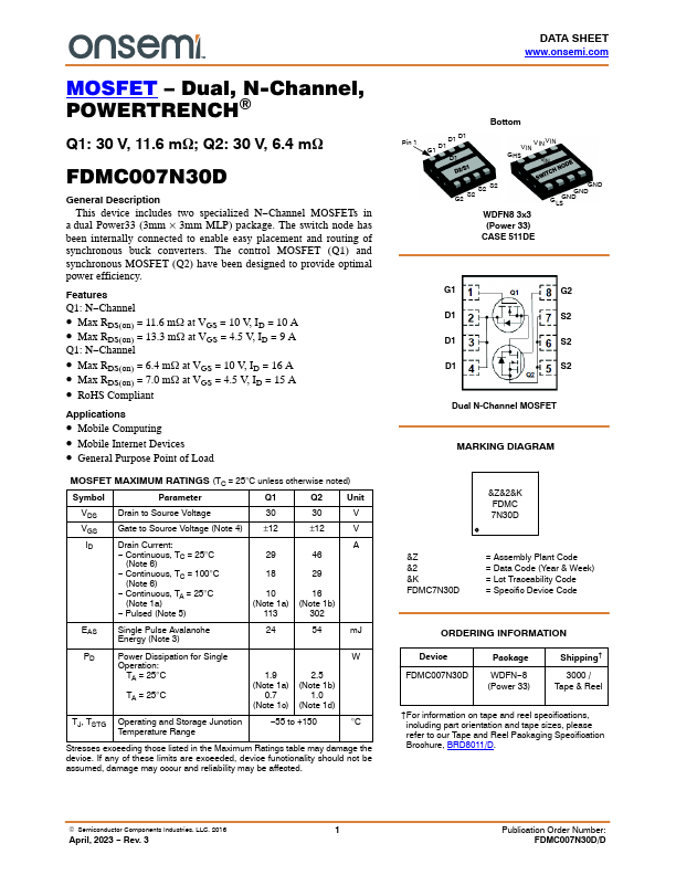
This device includes two specialized N−Channel MOSFETs in a dual Power33 (3mm × 3mm MLP) package. The switch node has been internally connected to enable easy placement and routing of synchronous buck converters.| Part No. | FDMC007N30D |
|---|---|
| Datasheet | FDMC007N30D Download |
| Manufacturer |  onsemi |
| Description | Dual N-Channel MOSFET |
| Buy | Stock & Price |
GENERAL DESCRIPTION
The control MOSFET (Q1) and synchronous MOSFET (Q2) have been designed to provide optimal power efficiency.FEATURES
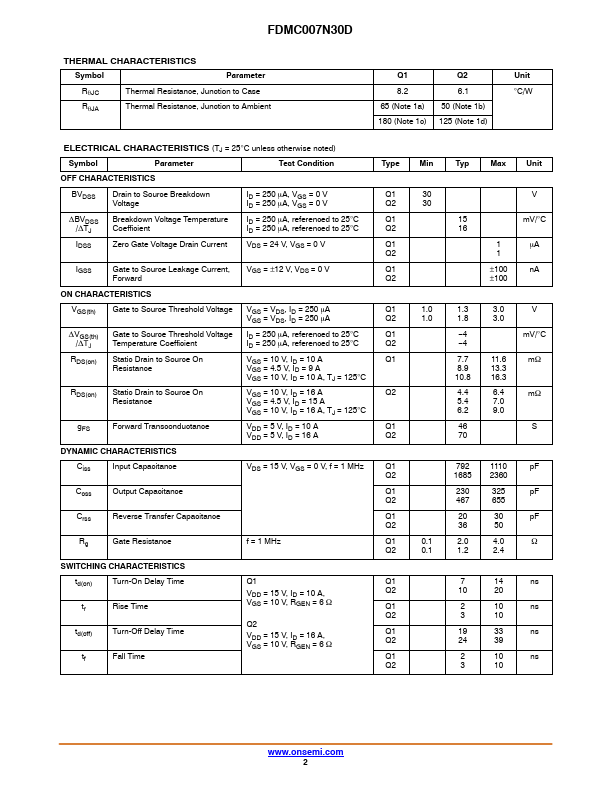
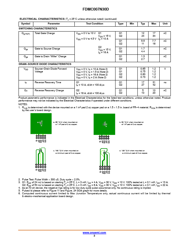
Q1: N−Channel● Max RDS(on) = 11.6 mW at VGS = 10 V, ID = 10 A
● Max RDS(on) = 13.3 mW at VGS = 4.5 V, ID = 9 A Q1: N−Channel
● Max RDS(on) = 6.4 mW at VGS = 10 V, ID = 16 A
● Max RDS(on) = 7.0 mW at VGS = 4.5 V, ID = 15 A
● RoHS Compliant
APPLICATIONS
● Mobile Computing● Mobile Internet Devices
● General Purpose Point of Load MOSFET
MAXIMUM RATINGS
(TC = 25°C unless otherwise noted) Symbol Parameter Q1 Q2 Unit VDS Drain to Source Voltage 30 30 V VGS Gate to Source Voltage (Note 4) ±12 ±12 V ID Drain Current: − Continuous, TC = 25°C (Note 6) − Continuous, TC = 100°C (Note 6) − Continuous, TA = 25°C (Note 1a) − Pulsed (Note 5) A 29 46 18 29 10 16 (Note 1a) (Note 1b) 113 302 EAS Single Pulse Avalanche Energy (Note 3) 24 54 mJ PD Power Dissipation for Single W Operation: TA = 25°C 1.9 2.5 (Note 1a) (Note 1b) TA = 25°C 0.7 1.0 (Note 1c) (Note 1d) TJ, TST...